Implementing Guardband Reduction Rules in High Volume Electronics Manufacturing Facilities
Dynamic guardbanding requires continuous fixture calibration and clear contract limits to recover false scrap yield without increasing customer DPPM defect risks.


Spread
Before releasing a batch to packaging, high-volume automated test lines clamp strict operational boundaries onto every component. These limits build in buffers well beyond whatever nominal specifications appear on the product datasheet. The gap between that catalog specification and the test program’s actual cutoff is the guardband.
Setting it requires balancing instrument calibration tolerances, probe interface drift, ambient floor temperatures, and internal heating across the automated test equipment’s pin electronics.
Static guardbands pegged at five or six standard deviations above measurement uncertainty keep out-of-specification parts from reaching buyers. But at volumes of a million units a month, that level of caution burns revenue. A measurement error of two percent on a high-frequency radio channel or power management unit quickly triggers false rejections.
Perfectly good silicon lands in scrap bins just because tester inaccuracy encroached on a legitimate silicon distribution operating near the specification edge.
| Uncertainty Parameter | Typical Standard Uncertainty | Distribution Model | Guardband Allocation Impact |
|---|---|---|---|
| Instrument Volumetric Calibration | ±0.15% of full scale | Normal (k=2) | Static shift across all DUT channels |
| Thermal Drift (15°C to 45°C) | ±0.35 mV per °C | Rectangular | Dynamic limit expansion required |
| Pogo Pin Contact Resistance | 15 to 80 mΩ per pin | Log-normal | Voltage drop variations under load |
| Cable Path Loss (5 GHz RF) | ±0.45 dB | Normal (k=2) | Direct gain specification contraction |
Calculating the statistical guardband requires combining individual uncertainty vectors per the ISO/IEC Guide 98-3 standard for measurement uncertainty evaluation. Take a power management integrated circuit with an upper voltage specification limit of 3.300 V. Paired with a high-speed digitizer carrying a combined expanded measurement uncertainty of 12.0 mV at a coverage factor of three, a conventional static setup subtracts that full uncertainty straight from the spec limit. That calculation leaves a conservative test cutoff of 3.288 V.
The combined standard uncertainty of an automated test line dictates the statistical width of false yield loss.
When the silicon process capability index stays tight, the true distribution of the silicon spans a narrower range than the tester accuracy window. Under a standard process distribution with a process capability index of 1.67, the die output operates comfortably inside the product specification. Applying static full-uncertainty guardbanding crops the upper portion of the yield curve.
Reducing guardbands without introducing field escapes requires transitioning from fixed mathematical subtractions to dynamic risk-based probability calculations defined in ANSI/NCSL Z540.3.
Trimming limits without calculating false acceptance risk, however, invites warranty disasters. If an automated test program tightens guardbands past the tester’s baseline drift thresholds, defective parts make it into the field. The landed cost of processing customer returns quickly dwarfs whatever was saved by not scrapping borderline dies.


Gage

Quantifying Automated Tester Measurement Repeatability
Every piece of measurement hardware injects variance into a production run. Pinning that variance down on automated test equipment requires formal Gage Repeatability and Reproducibility studies performed directly on the factory floor. Repeatability tracks the variation seen when one system measures identical devices using identical load boards.
Reproducibility captures the shift across multiple test channels, load board sockets, and operator shifts.
On high-speed semiconductor lines, mechanical socket wear and probe pin oxidation steadily eat away at repeatability. A Pogo pin displaying an initial contact resistance of 20 mΩ degrades to 150 mΩ after fifty thousand insertions. Under high-current pulse testing, that extra resistance creates parasitic voltage drops that corrupt parameter readings.
Routine automated calibrations zero out internal instrument drift, but they cannot fix an aging physical interface.

Fixture Parasitics and Socket Wear Mechanics
Physical test interfaces introduce signal reflections, inductive ground bounce, and stray capacitance. High-frequency analog devices experience gain attenuation when socket parasitic capacitance exceeds 0.5 pF per line. Guardband rules must account for the specific hardware degradation cycle of each test socket assembly on the handler.
Physical interface pin wear shifts contact resistance faster than internal instrument calibration drift.
- Socket Pin Inductance High pin inductance produces ground bounce during simultaneous output switching, artificially triggering low-voltage logic test failures.
- Thermal Gradient Drift Temperature differences between automated handler contacts and load board trace layouts shift analog bias currents during test sequences.
- RF Path Attenuation Constant flexing of flexible coaxial cables inside automated test heads degrades performance and introduces uncalibrated insertion loss.
- Relay Contact Contamination Oxide buildup on mechanical load-board switches causes intermittent open-circuit false rejections.
Without active fixture tracking, plants often widen their static guardbands just to absorb interface wear, masking deferred maintenance behind scrap yield rates. High-volume manufacturing plants reduce guardbands by enforcing strict interface replacement schedules tied directly to insertion counts rather than calendar time.
Test floors operating without continuous fixture tracking routinely blame silicon wafer foundries for lot-to-lot yield drops. Test engineers present log files showing parameter drift, attributing shifts to process instability rather than fixture wear. The assembly facility accepts load board replacement costs only after independent bench testing confirms the tester interface caused the variance.


Variance

Thermal Shift Mitigation across Multi-Site Automated Test
Thermal variations across multi-site test heads cause spatial measurement drift during high-throughput runs. An automated test handler screening sixteen device sites simultaneously exhibits localized thermal gradients up to 8°C across the load board plane. An uncompensated part tested at site one sees different thermal stress than a device tested at site sixteen, and the temperature coefficients of internal bandgap references cause voltage readings to drift across the board surface.
Thermal sensors embedded inside load board switch matrices supply continuous ambient data to the tester executive software. Real-time temperature compensation algorithms modify voltage force and measure limits based on active sensor feedback. This thermal compensation narrows the required guardband by eliminating ambient factory floor shifts from the uncertainty budget.

Should Test Limits Shift Dynamically with Wafer Lot Averages?
Wafer fabrication lots exhibit minor mean shifts within certified process windows. A static guardband treats every wafer lot identically, evaluating device parameters against absolute fixed boundaries. Dynamic Part Average Testing calculates moving statistical limits for each individual wafer or fabrication lot, computing the mean and standard deviation of parameter values across the first five hundred dies on a wafer.
| Rule Implementation | Upper Test Limit Offset | Lower Test Limit Offset | DPPM Risk Vector | Yield Recovery Delta |
|---|---|---|---|---|
| Static Six-Sigma Limit | USL – 6.0 standard deviations | LSL + 6.0 standard deviations | Below 0.1 DPPM | Baseline reference |
| Static Three-Sigma Limit | USL – 3.0 standard deviations | LSL + 3.0 standard deviations | 1.0 to 5.0 DPPM | +1.8% average yield |
| Dynamic Part Average (DPAT) | Wafer Mean + 6.0 Sigma | Wafer Mean – 6.0 Sigma | Below 0.05 DPPM | +2.4% average yield |
| Nearest-Neighbor Residual (NNR) | Spatial Spatial Median + 4.5 Sigma | Spatial Spatial Median – 4.5 Sigma | Below 0.01 DPPM | +3.1% average yield |
Parts landing more than three standard deviations away from the wafer mean face automatic rejection, even when operating within published specification limits. Flagging outliers this way isolates defective dies stemming from localized semiconductor processing flaws. Dynamic screening reduces the static guardband offset, capturing yield that static rules scrap.
Dynamic part average rules capture localized silicon anomalies without contracting the overall specification window for normal production.
Implementing dynamic parameter shift limits leaves open the question of defining absolute hard floor stops. If an entire wafer lot shifts systematically toward a specification boundary due to a process raw material change, dynamic limits shift accordingly. Programmers must decide whether to allow automatic limits to approach physical datasheet bounds without human intervention.
Binning
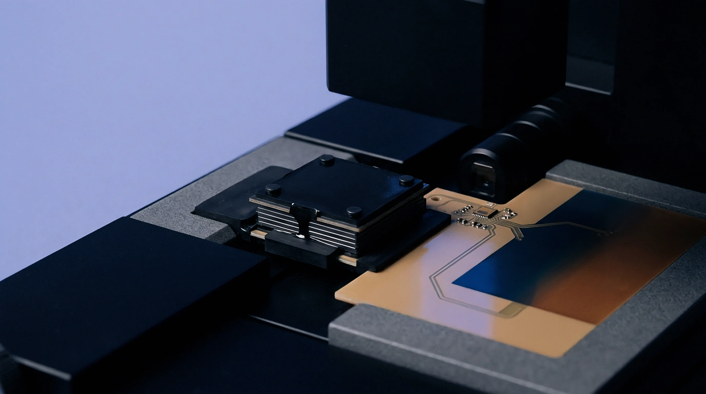
Automated test hardware assigns each tested component to a specific hardware or software bin based on test pass thresholds. Advanced binning software executes real-time statistical calculations on incoming parameter data streams. Instead of applying fixed upper and lower cutoffs across an entire production year, the system dynamically updates bin boundary conditions based on test system stability metrics and historical lot capability.
- Baseline characterization runs record fifty golden unit measurements across all available test sites to build reference distributions.
- Tester execution buffers live test data locally in Standard Test Data Format binaries.
- Robust median absolute deviation routines calculate outlier thresholds automatically, preventing bad die clusters from distorting moving means.
- Tester execution logic adjusts site-specific voltage force levels to cancel out trace attenuation identified during baseline runs.
- Final hardware bin assignment executes based on combined dynamic limit pass criteria, routing statistical outliers to diagnostic scrap bins.
High-volume radio frequency screening uses multi-tier adaptive binning to sort components into performance grade bands. A power amplifier module meeting tight error vector magnitude limits moves to a premium grade bin. A module demonstrating slightly higher distortion falls into a secondary commercial grade bin.
Reducing guardband width between performance bins maximizes the volume of high-value parts harvested from each wafer lot.
Contractual agreements specify that dynamic binning software modifications require formal customer change notifications under IATF 16949 standards.
Automated test programs operating adaptive binning rules store complete raw test records for every serial number. Standard industry quality clauses require keeping full test datasets accessible for five years. When field returns occur, engineering teams trace specific unit test values back to the exact socket, temperature, and dynamic limit applied during manufacture.
Under AEC-Q100 automotive guidelines, standard paragraph 4.2 dictates that any guardband reduction rule modifying statistical test limits must hold documented verification proof. The contract line obligates manufacturing facilities to halt adaptive limit adjustments whenever test system Gage Repeatability and Reproducibility ratios exceed ten percent.

Overkill
Scrapping functional silicon inflates unit costs directly. In high-volume operations running millions of parts, even a zero-point-five percent false reject rate discards tens of thousands of good silicon dies annually. Financial models balancing test overkill against test escape risk evaluate the total landed product cost across the device lifecycle.
Take an annual run of 10,000,000 wireless transceiver integrated circuits valued at $4.50 per unit packaging cost. Standard static guardbanding applies a strict 40 mV offset on receiver sensitivity measurements to guarantee a maximum field defect rate below 1 Defect Per Million (DPPM). Historical test line characterization proves tester combined uncertainty equals 8 mV.
The static guardband over-protects the test boundary by 16 mV beyond the necessary statistical confidence interval.
Yield loss attributed strictly to the 16 mV excess guardband measures 0.85% across the annual wafer volume. This scrap rate equates to 85,000 discarded units per year, representing $382,500 in direct lost product value. Transitioning to dynamic risk-adjusted guardbanding narrows the offset to 24 mV.
The reduction recovers 68,000 units, generating $306,000 in net annual yield recovery after accounting for software licensing and calibration costs.
Recovering false scrap through risk-adjusted test limits directly improves gross profit margins on high-volume packaged devices.
- Unit Cost Margin Impact High unit assembly costs turn false yield rejections into immediate financial scrap write-offs.
- Field Failure Liability Risk Shrinking guardbands too far increases customer field return costs, warranty claims, and line-stop penalties.
- Automated Tester Time Cost Complex dynamic guardbanding algorithms add millisecond calculation delays per device, consuming expensive ATE time.
- Customer Brand Degradation High-profile customer assembly line failures permanently damage supplier qualification status.
Yield recovery calculation models must account for test system execution overhead. Running complex matrix operations for spatial wafer correlation inside the test executive extends device cycle times. On high-speed handlers, adding ten milliseconds of algorithm processing per device increases operational costs by thousands of dollars per test floor month.
The economic benefit of guardband reduction exists only when yield recovery financial gains outweigh added test time charges.
A conservative rule of thumb dictates that guardband reduction projects should only proceed when false rejection cost exceeds tester modification expense by a factor of four.


Custody
Contractual Boundary Definition for Test Escapes
Transferring a semiconductor design package to an outsourced assembly and test facility introduces complex liability boundaries. When a product owner provides custom test limits and guardband definitions, the assembly factory executes the program strictly as delivered. If out-of-specification devices ship to end buyers due to inadequate guardbands written into vendor-supplied code, responsibility rests entirely with the product design house.
Subcontract test facilities frequently modify default guardband limits to improve reported factory yield figures. Master service agreements must establish strict configuration management protocols over test software repositories. Any local modification to test limits, force values, or wait times without signed Engineering Change Orders invalidates yield guarantees and shifts field failure financial liability to the factory operator.

Source Code Ownership in Automated Test Packages
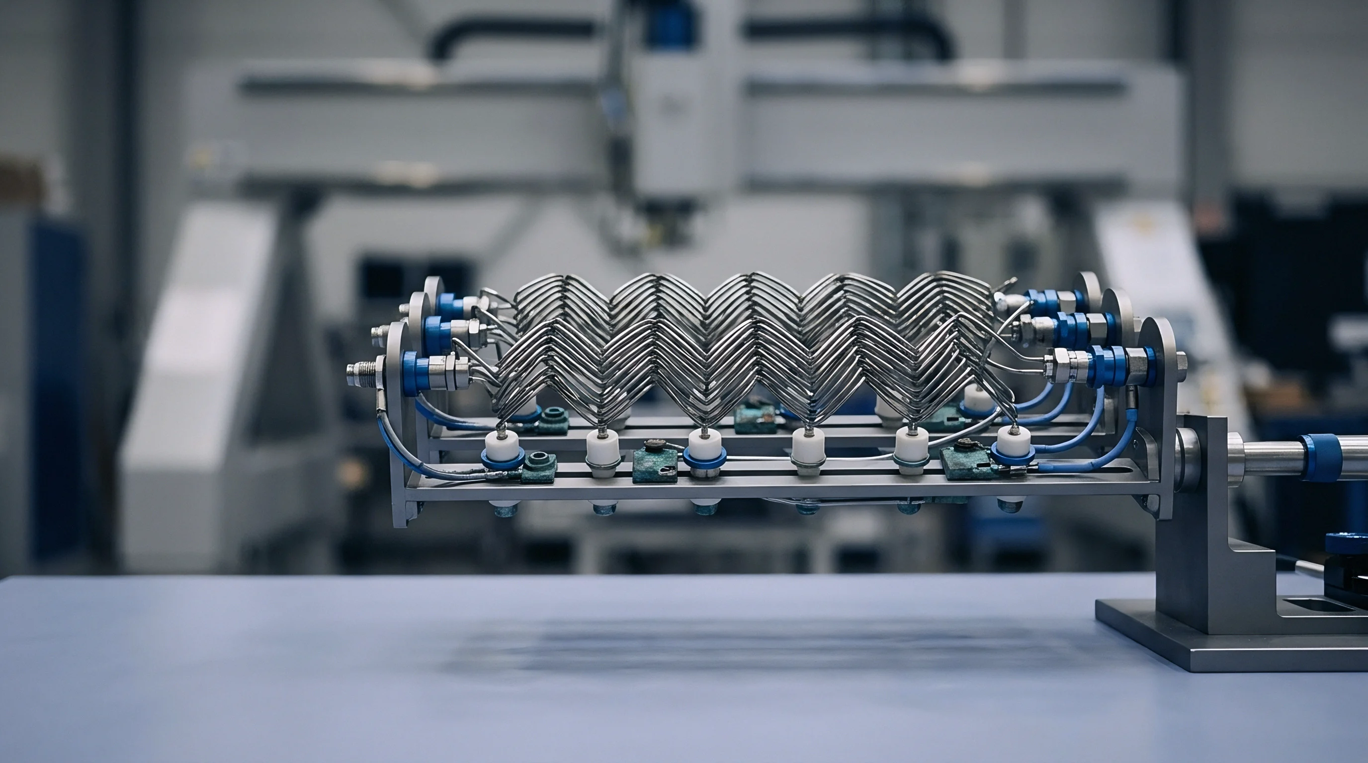
Automated test packages comprise physical load board schematics, FPGA timing files, dynamic link libraries, and high-level test executive scripts written in C++ or Python. Outsourced test facilities often treat customized calibration algorithms and dynamic limit modules as proprietary background intellectual property. Product owners must secure full source code ownership rights to all test routines created under Non-Recurring Engineering contracts.
Re-qualifying a high-volume product at a secondary outsourced assembly factory requires transferring the complete test dossier. If the original manufacturing facility retains exclusive ownership of dynamic guardband code, the product owner faces months of custom development to replicate test routines. Complete handover documentation includes raw calibration matrices, fixture board stack-up Gerber files, socket insertion tracking routines, and raw dataset parsing scripts.
Establishing full ownership of test program source code allows product teams to audit test limit logic independently. Third-party quality auditors review test executive code against mathematical guardband models to ensure compliance. Clean legal and technical handover practices enable product owners to dual-source manufacturing across global test locations without suffering yield drops or field quality spikes.