Automated Contact Interface Boards for Semiconductor High Volume Testing
Automated test interface board sourcing requires explicit transfer of artwork files, mechanical coplanarity tolerances, and contact wear thresholds.

Pin
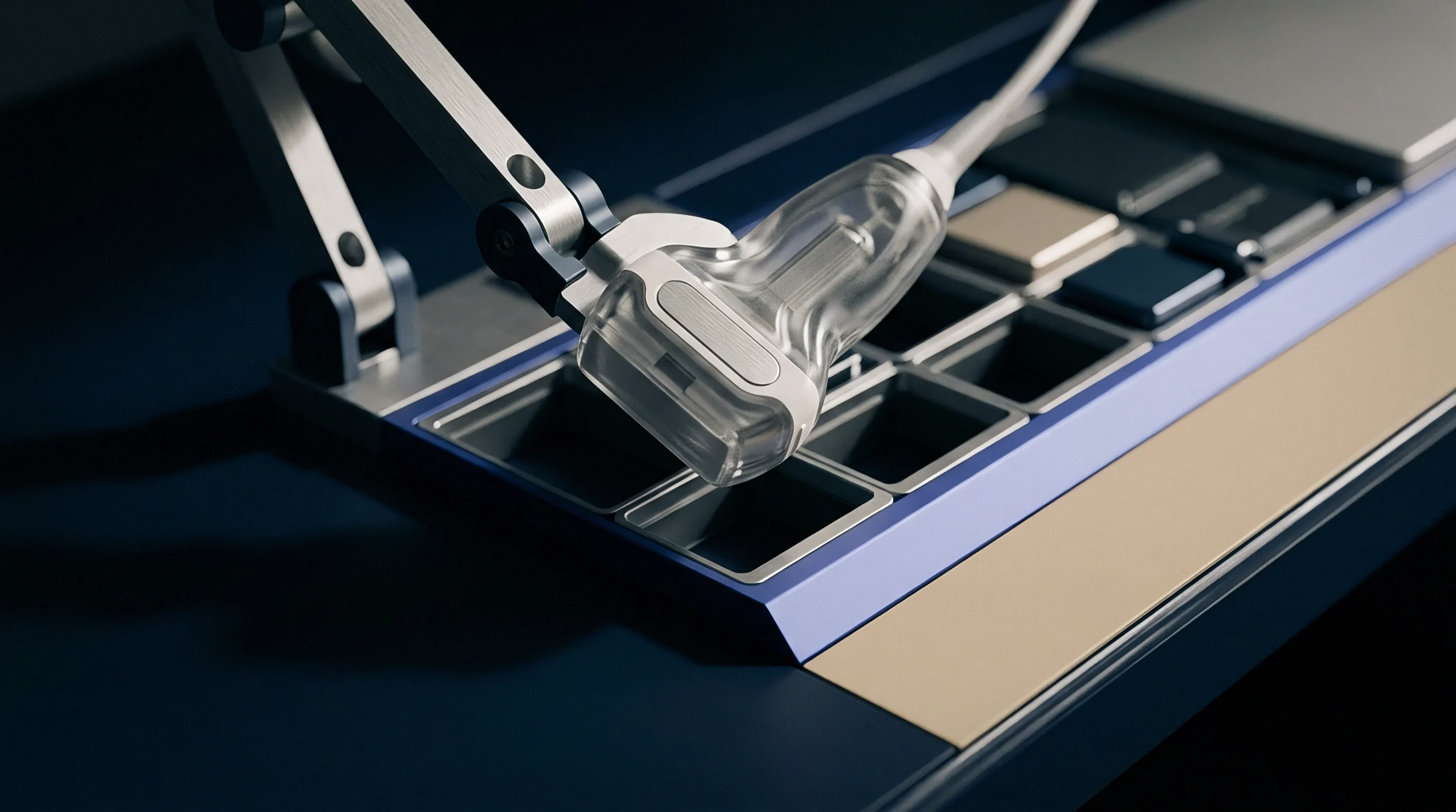
Automated test equipment relies on physical interface structures to bridge high-speed tester electronics and delicate semiconductor device pads. Micro-cantilever structures, vertical spring probes, and elastomeric contactors carry electrical signals across physical gaps ranging from several millimeters down to hundreds of micrometers. Mechanical spring force maintains solid metallic connection during high-speed device handler index cycles.
Touchdown force drops over time.
Device under test socket geometry dictates force transmission. Spring probes generate between fifteen and thirty grams of force per channel at nominal working height to break through surface oxide layers. Micro-cantilever structures use lateral sliding motion to penetrate native aluminum oxide or tin-lead intermetallics on wafer bond pads.
Pitch dimensions below 0.35 millimeters restrict spring wire diameters, limiting maximum achievable normal force without permanent plastic deformation.
Dynamic contact resistance varies directly with tip shape, vertical travel, and surface contamination. Oxide layers increase contact resistance. Initial engagement produces metallic micro-weld junctions across surface asperities.
Continuous cycling leads to tip geometry dulling, shifting the force-displacement curve away from nominal limits.
Dynamic contact resistance remains below fifty milliohms only when scrub depth exceeds twenty-five micrometers during touchdown.
Mechanical Contactor Force and Scrub Kinematics
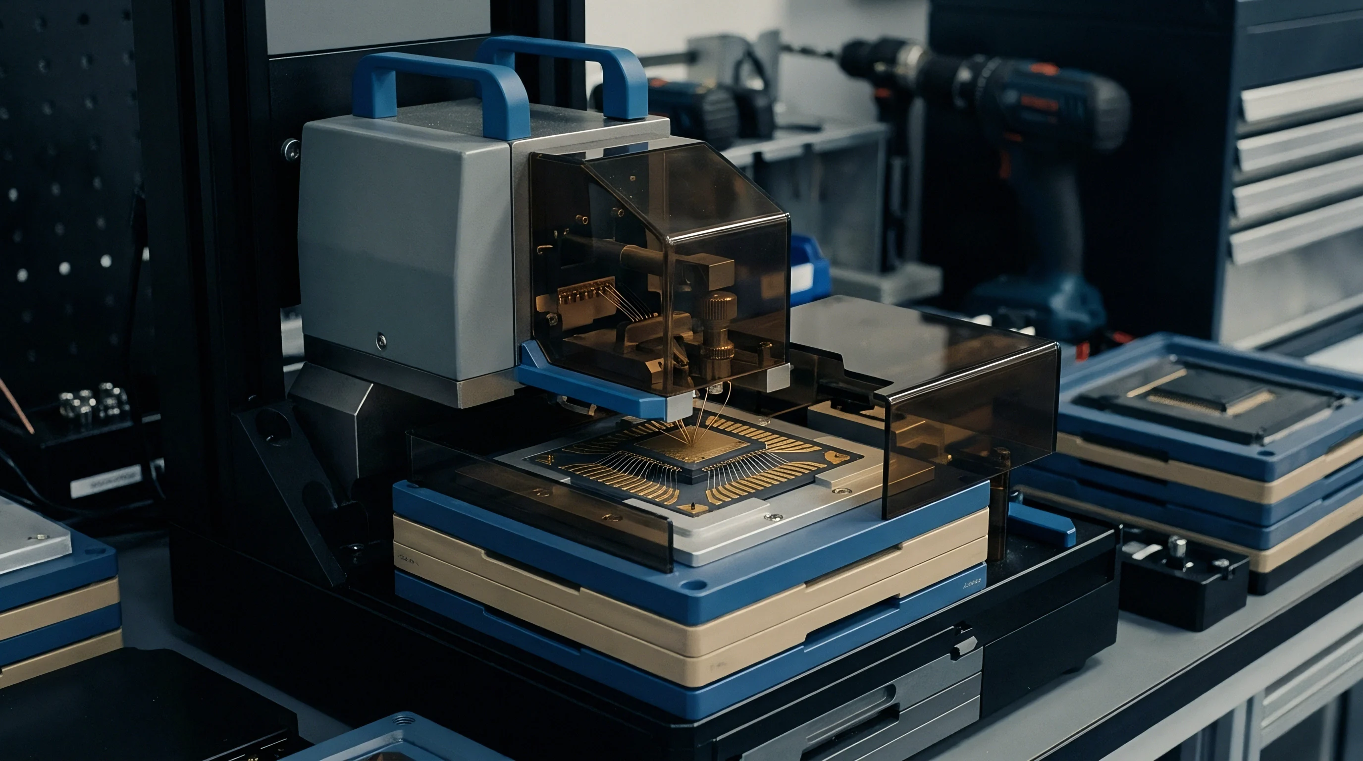
Electromechanical test interfaces convert z-axis handler travel into predictable contact wipes. Precision guide plates limit tip deflection to prevent shorting against adjacent signal pins in high-density grid arrays. Direct alignment pins enforce structural registration within five micrometers across twenty-inch interface boards.
Force displacement curves shift as spring elements experience cycle fatigue. Excessive vertical overdrive damages package substrates, while insufficient compression causes open circuits during test execution. Scrub kinematics require controlled lateral displacement to clean the contact patch without driving metallic debris into adjacent socket cavities.
| Contactor Architecture | Minimum Pitch (mm) | Normal Force per Pin (g) | Bandwidth at -1dB (GHz) | Current Carrying Capacity (A) |
|---|---|---|---|---|
| Vertical Spring Probe | 0.40 | 20 to 25 | 12 to 18 | 1.5 |
| Elastomeric Conductive Column | 0.30 | 10 to 15 | 40 to 60 | 0.8 |
| Micro-Cantilever Wire | 0.15 | 3 to 8 | 8 to 14 | 0.5 |
| Membrane Contact Array | 0.10 | 2 to 5 | 70 to 90 | 0.3 |

Contact Resistance Stability across Thermal Cycles
Temperature shifts from minus forty degrees Celsius to one hundred fifty degrees Celsius induce thermal expansion mismatches between organic print boards, metallic stiffeners, and ceramic sockets. Differential expansion alters probe positioning relative to device landing pads, altering electrical contact quality.
Material choices decide environmental survival. Beryllium copper and palladium alloy probe materials maintain spring modulus at high operating temperatures, whereas standard copper-zinc alloys exhibit stress relaxation. Plating thickness determines operational life under thermal cycling.
Unresolved structural deflection during extreme temperature cycling leaves open whether custom stiffener materials fully compensate for thermal expansion mismatches across large-area load boards.


Topology
Signal paths across high-density test interface printed circuit boards demand rigorous transmission line management to preserve edge rates below twenty picoseconds. Layer stackup configurations alternate high-speed differential signal layers with solid copper reference planes to suppress broadside coupling and common-mode radiation. Impedance mismatches create signal reflections.
Dielectric selection influences signal attenuation at high microwave frequencies. Advanced glass-weave materials using low-dissipation-factor resin systems maintain dielectric constant uniformity across multi-layer designs exceeding forty layers. Core thicknesses down to two mils prevent board warpage under mechanical clamping loads.
Power distribution networks require internal plane layers featuring low loop inductance to support high-current transient steps. Embedded capacitance layers situated adjacent to core supply planes damp high-frequency voltage ripple before energy reaches device power pins.
Impedance Matching and Path Discontinuities
Printed traces transitioning through vertical via structures experience capacitive parasitics due to catch-pad geometries and ground-plane antipads. Back-drilling eliminates unused via stubs that create resonant signal reflections at microwave frequencies. Back-drilling removes parasitic stub capacitance.
Controlled-impedance traces maintain fifty-ohm single-ended and one-hundred-ohm differential target values within three percent tolerance limits across entire fabrication panels. Trace width adjustments compensate for etching variations across thick outer copper foils.
- Differential Pair Routing maintains tightly coupled trace symmetry to eliminate skew and minimize common-mode signal conversion.
- Antipad Optimization removes reference plane copper around high-speed via transitions to reduce localized parasitic capacitance.
- Ground Via Shielding places perimeter return vias along differential traces to control characteristic impedance and isolate crosstalk.
- Via Stub Removal employs back-drilling depth control within fifty micrometers to suppress high-frequency signal resonances.
Power Distribution Integrity for High Current Devices
Automated test hardware delivers several hundred amperes to advanced system-on-chip devices during parallel functional screening. Multiple dedicated copper power planes decrease direct-current resistance from tester power supplies to socket terminals.
Decoupling capacitor placement directly beneath contactor socket footprints minimizes loop inductance. Low equivalent series resistance ceramic capacitors placed in ultra-small package sizes handle high-frequency current demands, preserving rail voltage stability under peak load conditions.
A continuous reference plane adjacent to every signal layer preserves transmission line impedance stability better than high-density trace routing crammed across divided split planes.
Wear
High-volume manufacturing sites execute millions of device contact cycles per month on individual test interfaces. Mechanical scrubbing wears down protective gold plating, exposing underlying nickel barrier layers to ambient atmosphere and solder contamination. Debris buildup degrades signal path integrity.
Intermetallic transfer accelerates terminal degradation. Lead-free tin-silver-copper solder bumps deposit soft tin particles onto spring probe tips during engagement. Tin oxides build up quickly, converting low-resistance metallic contact points into highly resistive semiconductor junctions.
Cleaning cycles delay production testing. Maintenance protocols rely on abrasive cleaning media embedded with aluminum oxide particles to strip accumulated tin debris from probe tips. Excessive abrasive cleaning shortens spring pin operational lifespan by stripping protective outer plating.
Plating integrity degrades rapidly once debris accumulation alters the normal force of the spring probe.

Can Offline Cleaning Restore Dynamic Contact Resistance?
Automated cleaning inline uses specialized cleaning polymers mounted in package hardware format to collect loose particulates without removing boards from tester heads. Dynamic contact resistance spikes indicate the need for intensive offline maintenance involving ultrasonic chemical baths and microscopic probe inspection.
Chemical solvent baths strip organic flux residues without degrading internal spring lubricants or housing polymers. Solvents fail to remove bonded tin-nickel intermetallic compounds formed under high electrical current densities.
| Insertion Count | Degradation Mechanism | Measured Parameter Impact | Corrective Action |
|---|---|---|---|
| 50,000 | Surface debris collection | Contact resistance drift (+15 mΩ) | Online elastomer pad wipe |
| 200,000 | Tin transfer to probe tip | Yield drop on analog pins | Offline brush and solvent clean |
| 500,000 | Gold plating wear-through | Intermittent open circuits | Offline abrasive tip rebuild |
| 1,000,000 | Spring stress relaxation | Normal force drops below 60% | Complete contactor element replacement |
Debris Accumulation and Material Transfer Mechanics
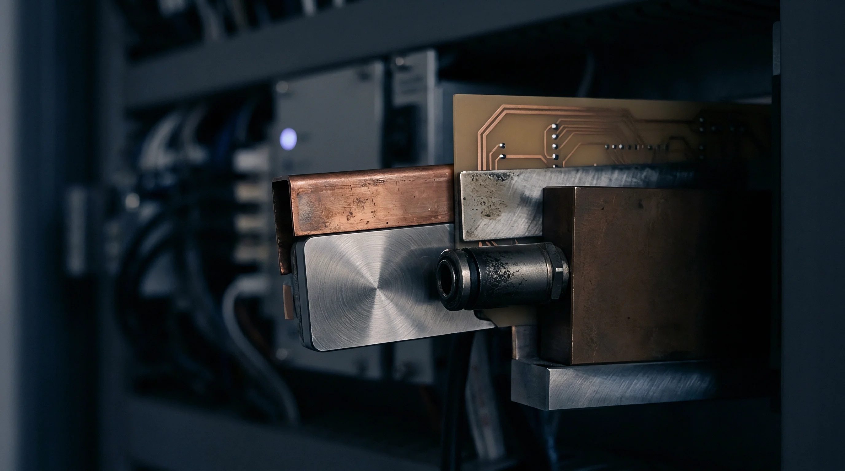
Particulate movement follows localized stress fields generated by probe tip geometry. Sharp crown probes pierce solder oxides effectively but trap loose debris inside center recessed points. Spear points shed debris easily but experience faster tip blunting.
Plating wear exposes raw nickel to moisture, triggering nickel oxide formation. Nickel oxide creates non-linear current-voltage characteristics that ruin analog precision measurements during parametric device testing.
- Inspect contactor socket under optical microscope at fifty-times magnification to audit particulate contamination patterns.
- Measure electrical continuity across all channels using automated loopback diagnostic hardware.
- Apply ultrasonic bath cycle with isopropyl alcohol solvent for fifteen minutes to dislodge loose debris.
- Perform mechanical force-displacement measurement on selected probe pins to verify spring return force.
- Record post-cleaning dynamic contact resistance baseline data inside factory maintenance log files.
Neglecting scheduled contactor cleaning leads directly to false device test rejections, artificial yield loss, and ruined production capacity across test cells.

Bringup
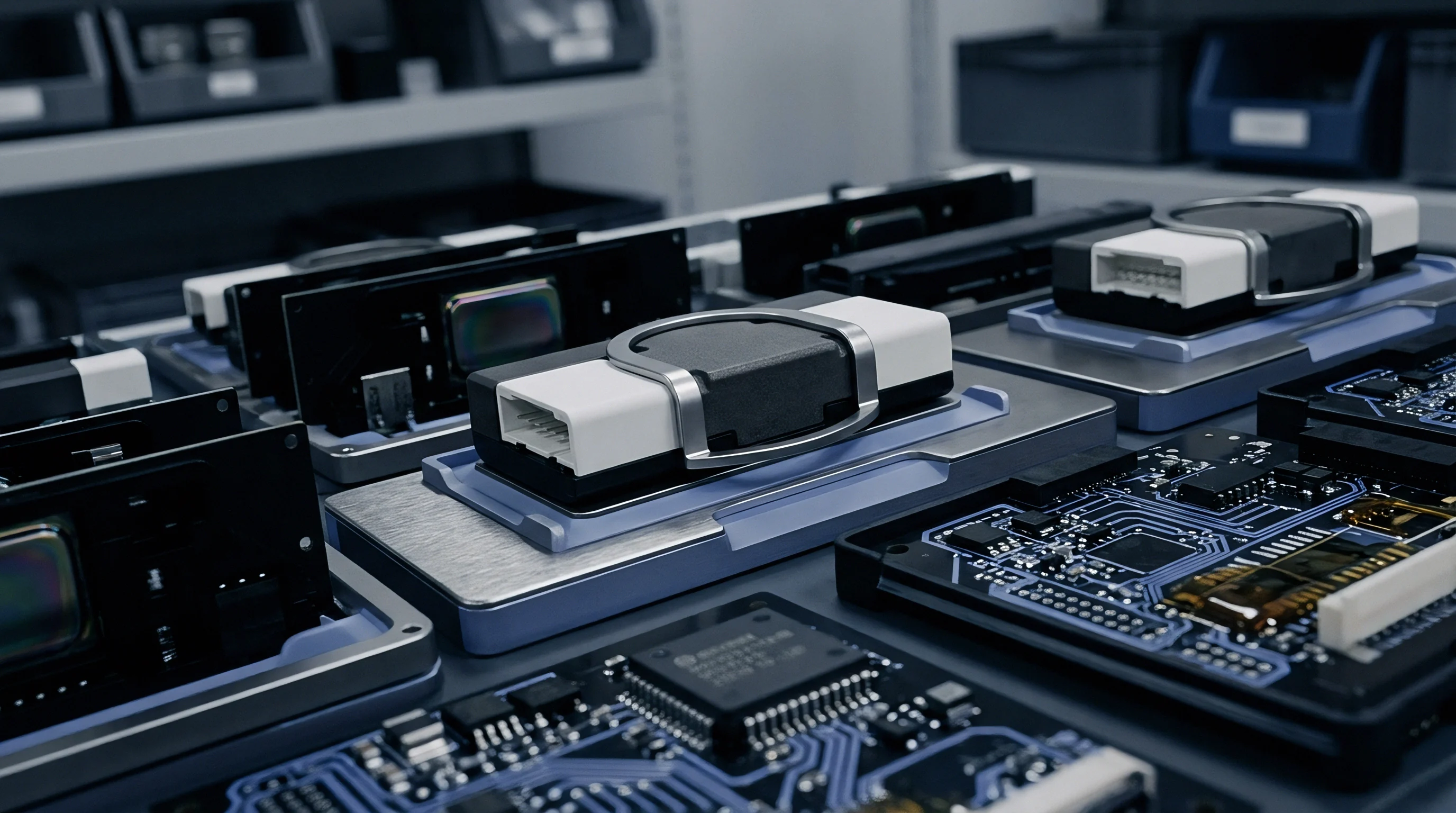
Hardware validation verifies that custom test boards meet tight signal integrity, power delivery, and mechanical planarity specifications prior to release for high-volume device production. Diagnostic loopback cards mount directly onto socket interfaces to simulate integrated circuit loads. Diagnostics verify hardware loopback paths.
Time-domain reflectometry maps impedance profiles across every trace length, flagging trace narrowing, poor via transitions, or ground plane breaks. Vector network analyzers confirm insertion loss and crosstalk limits across high-frequency differential pairs up to fifty gigahertz.
Gold-unit device verification compares parametric test data gathered on new load boards against historical baseline metrics established on reference hardware. Discrepancies point toward board fabrication errors, incorrect passive component values, or assembly soldering defects.
Acceptance signoff under ISO 9001 change control requires full electrical time-domain reflectometry trace datasets for every production board shipment.

Diagnostic Verification and Loopback Integration
Loopback fixture design mirrors target package pinouts while connecting driver channels directly to receiver channels through precision attenuation networks. System firmware executes self-test procedures to confirm channel continuity and timing alignment across all tester resources.
Calibration records confirm baseline performance. Thermal chamber testing verifies loopback path stability across expected production environment temperature ranges. Board warpage under thermal load causes contact separation inside loopback interfaces, triggering false diagnostic failures.

Design Transfer Dossier and Signal Calibration
Design handover requires full native artwork documentation, fabrication stackup detail, assembly drawings, and automated test parameter lists. Incomplete design packages force manufacturing sites to guess critical stackup tolerances, resulting in out-of-spec trace impedance on re-ordered boards.
Part-change notifications control component substitutions on test interfaces. Unapproved substitution of low-ESR bypass capacitors with standard commercial passives introduces power rail noise, corrupting sensitive analog device measurements.
The vendor claims that trace length matching within five mils renders differential skew negligible, ignoring dielectric constant variations across large circuit board panels.

Settlement
Procurement models for automated test hardware balance internal engineering resources against vendor non-recurring engineering charges. Turnkey development places complete design, layout, thermal analysis, and verification responsibility onto the interface vendor. Turnkey contracts assign design risks.
Semi-custom integration allows internal test engineering teams to complete schematic design while outsourcing complex multi-layer board layout, signal integrity simulation, and mechanical stiffener design. Reference design execution copies vendor baseline layouts directly, shifting risk back to internal bring-up teams when target board layouts deviate from reference standards.
NRE fees cover custom layout hours. NRE invoices separate mechanical tooling, signal integrity simulation, fabrication test vehicle generation, and diagnostic software creation into distinct billing items to clarify ownership boundaries.
Commercial Scope and Engineering Ownership Boundaries
Contractual terms fix ownership rights for physical manufacturing files, including Gerber X2 outputs, drill tables, and component placement coordinates. Buyers retaining full artwork ownership can send re-orders to alternative board fabrication facilities without paying secondary design fees.
Intellectual property clauses govern socket contactor geometry and custom stiffener mechanics. Vendor-owned mechanical designs lock buyers into single-source spare pin and maintenance component procurement regimes.
| Integration Level | Engineering Ownership | Deliverable Dossier Scope | NRE Cost Basis | Unit Cost Impact |
|---|---|---|---|---|
| Turnkey Custom | Vendor design, Buyer usage rights | Gerber outputs, FAT reports, physical boards | High ($40k – $90k) | Low (Amortized over volume) |
| Semi-Custom | Joint ownership by block | Schematics, layout files, simulation models | Medium ($15k – $40k) | Moderate |
| Reference Build | Buyer owns modified files | Raw CAD files, complete BOM, mechanical drawings | Low ($5k – $15k) | High (Small production batch) |
| White-Label Standard | Vendor full ownership | Finished assemblies, generic pin maps | Zero | Fixed catalog price |
Cost Amortization and Spares Maintenance Strategy
High-volume manufacturing accounting balances upfront board development expense against per-unit test costs. Tooling costs for specialized mechanical stiffeners and high-density probe head sockets amortize across projected device shipping volumes.
Spare parts strategy requires stocking fully assembled spare contactor sets, individual replacement spring pins, and extra alignment guide plates directly at test facilities. Spare contactors limit line downtime. Rapid-repair service level agreements compel vendors to return rebuilt test interfaces within forty-eight hours of socket fatigue failure.
Unclear ownership of Gerber master files shifts the total financial burden of downstream board re-spins entirely onto the buyer.
Standard supply agreements incorporate IPC-6012 Class 3 performance standards, obligating vendors to replace any interface board that exhibits inner-layer micro-cracking or dielectric delamination during normal production operation.