Meaning
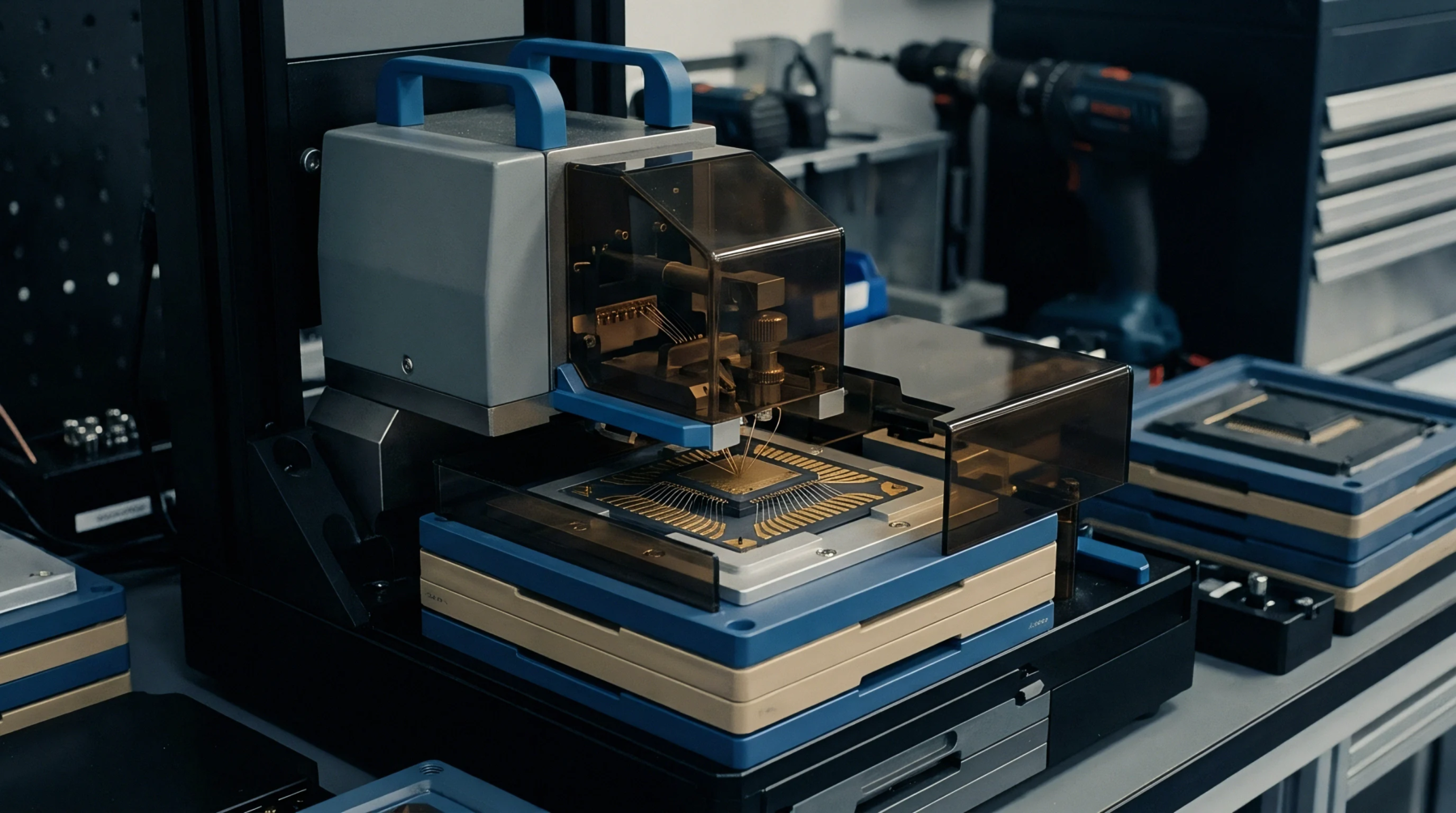
Simultaneous verification of multiple individual semiconductor die or hardware components on a single wafer or panel allows for higher throughput during the production stage. This multi site testing technique reduces the total time required for final device evaluation by engaging parallel pathways for signal input and output. The equipment synchronizes parallel stimulus delivery across various sites to ensure each individual unit undergoes an identical sequence of functional checks.
Efficiency gains scale with the number of sites active, though the physical constraints of the probe card and the available interface channels determine the upper limit of the array.
Parallel Architecture
Throughput optimization relies upon the capacity of the test head to handle increased data volume without stalling the hardware. Integrated circuits often require high pin counts for power, ground, and high-speed signal integrity. When the interface board divides these resources among several sites, the total load per pin must remain within the thermal and electrical tolerance of the tester channels.
Proper alignment of probe needles against the die pads becomes harder as the number of sites increases because mechanical tolerances tighten across a wider surface area. A well-designed setup ensures that cross-talk between signal lines stays below the noise floor so that one failing unit does not introduce errors into the measurements of neighboring functional devices.
Interface Constraint
Hardware limitations frequently dictate the density of testing sites on a carrier or wafer. The physical footprint of each contactor socket consumes board area, leaving less space for bypass capacitors and decoupling elements that stabilize power delivery. If the voltage drops during simultaneous switching of outputs at many sites, the resulting noise threatens to corrupt data accuracy.
Designers manage this risk by balancing the impedance of the signal paths and placing sensitive analog components at a distance from digital high-speed lines. Scaling beyond current limits demands smaller interconnections and more complex routing strategies to maintain signal fidelity across the entire test platform.
Economic Consequence
Capital equipment amortization costs decrease as the volume of devices processed per hour climbs. Reducing the duration of the test sequence minimizes the overhead per unit, which yields lower total manufacturing costs for the product. Fixed costs for test hardware remain high due to the complexity of the probe card, yet the reduction in cycle time justifies the investment for high-volume consumer electronics.
Market demand for cheaper hardware persists, forcing manufacturers to adopt ever more aggressive site counts. Each added site shortens the product lifecycle lead time by accelerating the transition from raw wafer to qualified component.