Resolving Substrates and Firmware Binary Divergence in Dual Sourced Wireless Module Manufacturing Package Files
Dual sourced wireless module manufacturing package files require synchronized substrate stackups and hardware sensing firmware to resolve binary divergence.
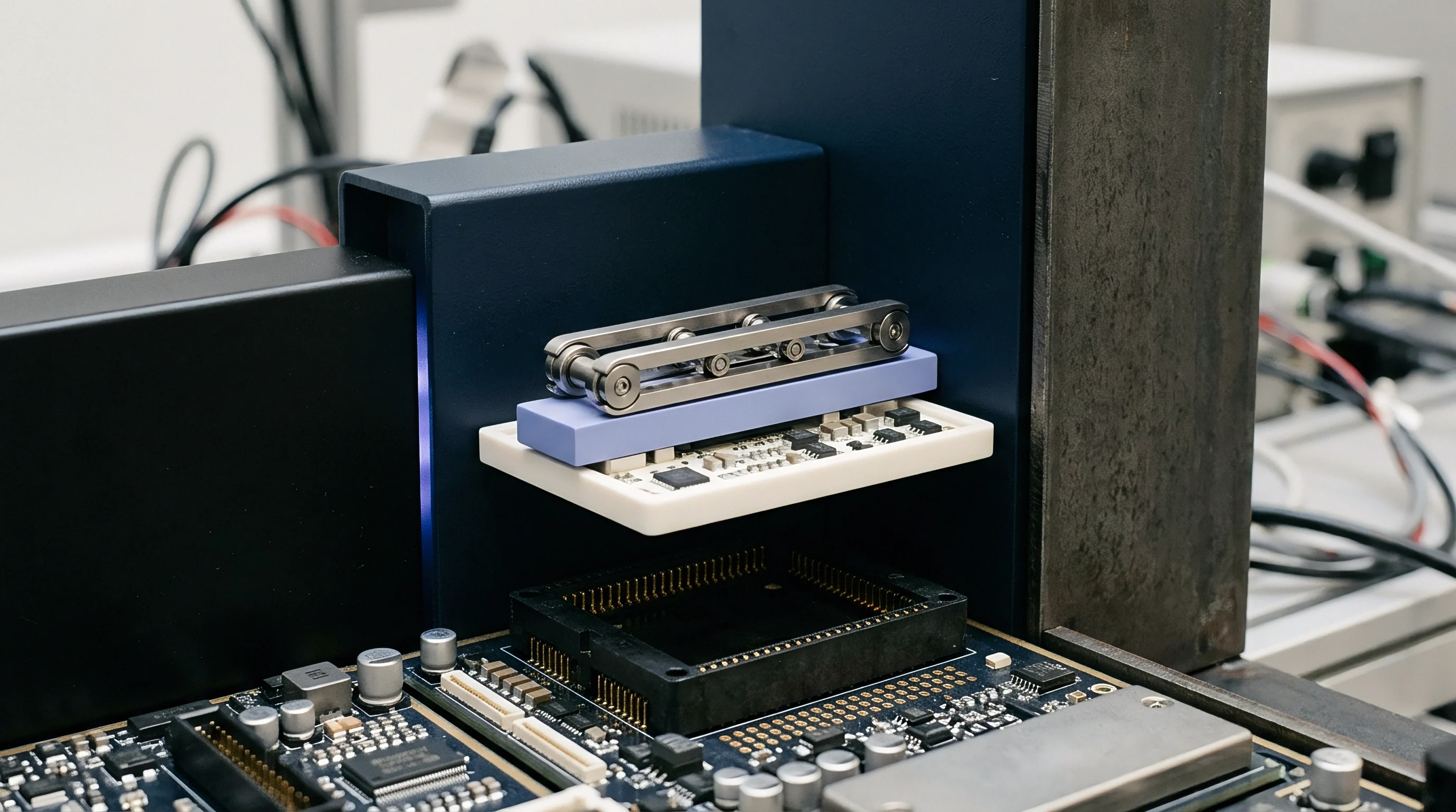

Substrate
Dielectric variations across laminate suppliers alter trace impedance and RF propagation characteristics in high-frequency module layouts. When dual-sourcing wireless hardware, primary assembly plants often rely on specific woven-glass epoxy substrates, whereas secondary manufacturing facilities select alternative resin matrices to optimize local material supply chains. A layout tuned for a primary laminate with a dielectric constant of 3.6 at 2.4 gigahertz encounters severe return loss penalties when replicated on a secondary laminate exhibiting a dielectric constant of 4.1.
The physical width of a fifty-ohm microstrip or grounded coplanar waveguide changes directly with substrate permittivity, board stackup thickness, and copper foil roughness. Ignoring these physical parameters during manufacturing package consolidation introduces RF mismatch, increased insertion loss, and harmonic distortion on antenna feedlines.
Evaluating transmission line impedances under IPC-TM-650 test methods catches board-level discrepancies early. Layer stackup adjustments between fabrication sites also shift the reference plane distance for critical RF traces. A reduction in core layer thickness from 100 micrometers to 80 micrometers compresses the capacitance between signal paths and ground planes, altering trace inductance ratios and quickly undermining assembly yield.
Pinout remapping and land pattern discrepancies compound the physical divergences between manufacturing sites. Component package footprints designed for high-density interconnect designs require microvia structures, buried vias, or blind via arrays. Secondary fabricators may lack the mechanical drilling resolution or laser ablation accuracy needed for staggered microvia configurations, prompting localized pin reassignments or land pad enlargement.
Expanding land pad dimensions by twenty micrometers alters parasitic capacitance at high-frequency transceiver pins, detuning input matching networks and shifting center frequencies.
| Laminate Designation | Dielectric Constant (10 GHz) | Dissipation Factor (10 GHz) | Coplanar Waveguide Width (50 Ohm) | Impedance Tolerance Range |
|---|---|---|---|---|
| 3.72 | 0.0085 | 0.210 mm | +/- 4.2 Ohms | |
| 4.15 | 0.0160 | 0.178 mm | +/- 6.1 Ohms | |
| 4.35 | 0.0185 | 0.165 mm | +/- 7.0 Ohms | |
| 3.48 | 0.0038 | 0.232 mm | +/- 2.8 Ohms |
RF Trace Impedance Shift across Laminate Suppliers
High-frequency signal transmission lines depend on uniform dielectric properties throughout the circuit board substrate. Variations in glass weave styles, such as 106 versus 2116 glass cloth, introduce localized dielectric fluctuations known as the fiber weave effect. Traces running parallel to the glass bundle encounter periodic dielectric transitions, shifting phase velocities and skewing differential signal pairs.
Primary lines built on tight-weave materials exhibit uniform impedance profiles, while secondary lines using loose-weave laminates develop resonance peaks within operational frequency bands.
RF power transfer efficiency drops off steeply when return loss falls below fifteen decibels across the antenna matching network. Adjusting copper trace geometries through automated Gerber file modification script tools compensates for laminate permittivity differences. Fabricators modify outer trace etching widths by pre-calculated delta values derived from dielectric bench testing, preserving targeted waveguide impedances without altering internal routing layers.
RF trace geometry requires recomputation whenever laminate dielectric constants shift by more than five percent across board vendors.
Etch factor variations between production facilities introduce further geometric discrepancies on signal conductors. Chemical copper etching in automated conveyor lines produces trapezoidal trace cross-sections rather than rectangular profiles. A factory using heavy spray pressure generates steeper sidewall angles, narrowing the effective top width of transmission lines.
Top-width reductions raise trace inductance, detuning bandpass filters embedded directly into module substrate layers.

Package Footprint Variance in Pin Register Maps
Land pattern geometry directly affects surface-mount component alignment, solder joint reliability, and pinout register mapping. Dual-sourced wireless modules frequently utilize alternate land grid arrays or quad-flat no-lead leadframe structures tailored to regional manufacturing capabilities. Pin layout offsets occur when secondary packaging houses adapt original ball grid array locations to accommodate larger pad clearances or modified thermal relief structures.
A pin shift as small as one hundred micrometers breaks electrical compatibility with standard host board test jigs, causing physical bridging or open circuits during reflow soldering. Substrates designed with thermal vias directly under central exposed pads require controlled solder mask dams to prevent solder wicking into via barrels. Differences in solder mask tolerance between secondary manufacturing plants alter solder volume deposition, causing package tilting and coplanarity errors across peripheral signal pads.
Component displacement during reflow soldering introduces parasitic coupling between adjacent signal channels. High-density pin arrays positioned near sensitive low-noise amplifiers collect extraneous noise when pad structures overflow into adjacent ground fills. Establishing standardized IPC-7351 land pattern rules across all package release files locks outer pad dimensions, preventing uncoordinated modifications by local fabrication plants.
Localized dielectric substitutions often fall within industry-standard FR-4 manufacturing envelopes and meet baseline mechanical dimensions without altering raw board supply lead times.


Patch
Software abstraction layers decouple underlying hardware revision shifts from application software execution across dual-sourced assembly streams. When physical substrates diverge due to alternate pin assignments, transceiver revisions, or peripheral power management IC substitutions, low-level binary configurations require dynamic adaptation. Hardcoding peripheral memory addresses or peripheral pin multiplexing arrangements into a single static image causes boot failures or system instability when deployed on secondary module builds.
Implementing modular board support package overlays enables software execution engines to identify physical hardware parameters at initial boot stages.
Designing board support packages with dynamic hardware identifier queries isolates physical differences. Dynamic hardware identification relies on dedicated board revision pins, non-volatile memory flag registers, or electronic fuses burned into silicon during initial factory calibration. Low-level drivers query these hardware indicators before initializing system clocks, peripheral interfaces, or radio frequency front-end components.
Correctly reading hardware identification registers directs the software runtime environment to load matching register configuration maps without requiring separate firmware source branches for each manufacturing facility.

Hardware Abstraction Overlays for Dynamic Revision Sensing
Layering software abstraction structures separates low-level register control from core wireless stack functions. Board support packages utilize device tree structures or driver table pointers to map physical hardware registers to logical API calls. When a secondary manufacturing site installs an alternate radio frequency front-end chip with different control interfaces, the underlying abstraction layer handles command translation without altering top-level protocol stack code.
Misconfiguring power management integrated circuit rail sequences through incorrect low-level register writes causes immediate brownout resets during radio transmission bursts. Software abstraction overlays contain plant-specific power sequencing tables, enabling boot scripts to apply appropriate voltage step delays and current limits based on detected module hardware IDs.
Failure to meet IPC-2581 class three layer stackup definitions voids factory yield guarantees during dual site manufacturing transfers.
Driver initialization sequences check peripheral hardware ID registers during early boot cycles. If register reads return values assigned to secondary module builds, driver routines substitute memory-mapped register offsets dynamically. Dynamic substitution eliminates binary branching in host applications, allowing host devices to accept modules from either assembly site without updating host-level operating software.

Register Multiplexing Adjustments in Low Level Drivers
Pin multiplexing flexibility in modern microcontrollers allows single physical pins to route signals to internal peripherals such as serial communication blocks, timers, or pulse-width modulators. Substrate pin remapping between dual-sourced modules requires explicit re-routing of internal pin multiplexing registers within low-level driver initialization routines. Static driver implementations designed for primary layouts cause signal collisions or dead pins when executed on secondary substrate routing configurations.
Peripheral register configuration tables define pin routing based on detected module board revisions:
- Hardware Revision Registers ~ Reading physical strapping pins or electronic fuses at cold boot identifies the exact substrate revision and layout variant.
- Pin Multiplexing Overlays ~ Loading dynamic register map arrays rebinds peripheral functions to correct physical ball locations before turning on peripheral power rails.
- Clock Tree Allocation ~ Adjusting internal phase-locked loop multipliers accommodates alternate crystal oscillator frequencies mounted on secondary assembly lines.
- Radio Frequency Front-End Maps ~ Modifying general-purpose input and output logic assignments controls transmit and receive switches unique to secondary power amplifier modules.
Replacing an onboard microcontroller or wireless system-on-chip with an updated silicon stepping alters internal register definitions and peripheral base addresses. Low-level drivers must evaluate peripheral version identification registers embedded in silicon to apply appropriate register patches before initializing peripheral subsystems. Omitting these checks leads to unhandled bus faults when software writes to obsolete register offsets.
Manufacturing supply contracts explicitly mandate that any software patch or board support package adjustment intended to reconcile dual-source hardware divergence must maintain complete backward compatibility with reference host driver APIs and pass full regression testing suites before line deployment.


Binary
Executable binary alignment across dual-sourced module streams demands unified build flags, conditional execution vectors, and deterministic linker configurations. Packaging multiple hardware targets into a single distribution archive prevents factory line cross-contamination where incorrect software images are flashed onto physical substrates. Embedded bootloader architectures evaluate physical hardware parameters, validating target board identities before passing execution control to primary application vectors.
Structuring executable binary files with unified header structures allows factory automated programming tools to verify image compatibility before transferring image data into non-volatile memory.
Compiling target firmware images with unified linker flags across both assembly lines isolates memory regions dedicated to hardware-specific driver structures. Placing hardware-dependent configuration matrices within reserved non-volatile flash sectors prevents memory offset shifts across general application binaries. Application code accesses hardware parameters through fixed jump table locations or indirect memory pointers, ensuring identical binary execution across different physical modules.
Why Do Substrate Dielectric Variance and Pinout Remapping Trigger Bootloader Failures?
Bootloader software routines operate in restricted runtime environments before full system board support packages initialize. Substrate modifications altering pinout mapping affect critical early boot signals, including external flash chip-select lines, crystal oscillator enable pins, and hardware strapping lines. If a bootloader attempts to communicate with external SPI flash memory using primary pin assignments on a secondary substrate layout, serial communication fails, dropping the device into an unrecoverable boot loop.
When secondary substrates incorporate larger flash memory components to compensate for component shortages, bootloader memory partition boundaries shift. Flash page erase sizes and block alignment requirements alter image storage layouts. Bootloaders lacking dynamic flash geometry detection fail to locate application images, interpreting shifted execution vectors as corrupted memory regions.
A three hundred megahertz impedance mismatch on coplanar waveguides increases insertion loss by zero point eight decibels per centimeter at high temperatures.
Clock initialization timing discrepancies cause boot failures during cold temperature startups. Secondary modules featuring alternate crystal resonators require modified load capacitance settings and longer stabilization delay loops in bootloader code. Initiating high-speed internal phase-locked loops before external clock sources stabilize introduces clock jitter, corrupting early memory access cycles and halting bootloader progress.

Unified Image Compilation with Dynamic Linker Scripts
Compiling software images into unified, multi-target binary files eliminates the operational risk of flashing wrong firmware images during dual-source manufacturing runs. Linker scripts organize compiled binary layouts into distinct execution blocks, combining common core application logic with conditional hardware patch tables. Dynamic boot logic selects the correct patch execution path at runtime based on hardware detection flags.
Memory region overlap errors occur when conditional compilation flags inflate section sizes beyond allocated flash partition limits. Explicit linker placement directives enforce rigid memory boundary checks, throwing build errors during continuous integration stages if hardware driver additions exceed pre-allocated memory boundaries.
Executable image headers store cryptographic signatures, image length metrics, target hardware identifiers, and entry point addresses. Automated factory flashing software parses these headers before burning binaries to flash memory, rejecting images built for incompatible module revisions.
| Identification Mechanism | Hardware Sensing Overhead | Flash Memory Offset Shift | Execution Latency Delta | Boot Failure Probability |
|---|---|---|---|---|

Memory Map Partitioning for Dual Target Boot Vectors
Partitioning non-volatile flash memory accommodates dual-target boot structures while preserving fixed execution entry points for host microcontrollers. Allocating static memory blocks for bootloader code, hardware calibration tables, primary application images, and backup recovery images guarantees memory map stability across module revisions.
Aligning flash partition boundaries with physical flash block erase sizes optimizes write speed and extends flash endurance during over-the-air firmware updates. System configurations define execution vectors using relative addressing modes, permitting relocation of execution paths without rebuilding compiled binary source code.
Synchronizing firmware binary distributions across dual-sourced assembly facilities requires structured execution steps:
- Compile core application source modules into static object libraries to guarantee instruction sequence parity.
- Generate location-independent position-independent code blocks for hardware-specific low-level abstraction drivers.
- Execute linker scripts that enforce rigid flash memory partition boundaries and define fixed symbol lookup tables.
- Append cryptographic headers carrying specific target hardware revision masks and payload checksum signatures.
- Bundle primary and secondary binary target images into a single unified manufacturing archive file.
- Run automated binary analysis tools to verify target entry point offsets against standard hardware qualification specifications.
Calculating cyclic redundancy checks or cryptographic hash digests across full binary images ensures image integrity prior to execution. If a factory automated flash utility writes a binary image across an improperly aligned memory block, bootloader verification routines detect the mismatch, halting boot sequences to prevent partial execution cycles that can permanently damage RF power stages.
Deploying divergent binary files across dual-sourced production lines without dynamic hardware verification introduces high field recall costs, unrecoverable bootloader lockups, and severe line stoppage damages when host devices receive unbootable module packages.


Manifest
Package release archives govern the physical and logical artifacts delivered to dual-sourced manufacturing lines. A complete manufacturing release package contains fabrication Gerber files, drill files, bill of materials tables, pick-and-place coordinate data, assembly drawings, firmware binaries, and automated test scripts. When managing secondary manufacturing partners, version control procedures must maintain absolute synchronization between physical substrate revisions and compiled software binaries.
Distributing loose, unverified files directly to factory managers introduces configuration drift, where local plants build hardware using outdated Gerber layers or flash legacy firmware images.
Tracking binary checksum outputs across release archives during factory acceptance audits catches configuration drift before assembly. Containerizing build environments inside container images ensures bit-for-bit build reproducibility across geographically separated development centers and factory locations. Release archives packaged with cryptographic manifest signatures allow factory manufacturing execution systems to automatically extract, verify, and route assembly files to automated surface-mount lines without human intervention.

Fabrication Gerber Versioning and Bill of Materials Sync
Substrate design revisions alter physical Gerber X2 and IPC-2581 outputs, requiring explicit link mechanisms between fabrication layer data and bill of materials databases. An update to an outer copper layer that adjusts trace width parameters for local dielectric conditions requires a corresponding update to the master manufacturing package manifest file. If component references in pick-and-place files drift from corresponding bill of materials line items, automated placement machines drop components or select incorrect component package sizes.
Compiling firmware binaries on different host operating systems or toolchain build versions introduces binary variance, altering executable hash values. Enforcing containerized toolchains locks compiler versions, library dependencies, and linker behavior, guaranteeing identical binary outputs regardless of where package generation occurs.
Firmware bootloaders that query hardware configuration registers prevent execution halts caused by substrate pinout swaps.
Bill of materials files utilize approved vendor list records to define acceptable component substitutions for secondary assembly plants. Every approved vendor component must undergo electrical and physical verification testing to confirm parametric parity with primary components before entry into the master package manifest.

Automated Verification Pipelines for Packaging Integrity
Continuous integration pipelines automate package compilation, executing verification scripts before exporting delivery archives to external manufacturing partners. Automated testing scripts validate file completeness, parsing Gerber files for design rule compliance, checking bill of materials syntax, and verifying software binary compilation against target hardware rules.
Local manufacturing teams attempting manual script edits introduce silent build syntax errors that corrupt automated testing pipelines. Restricting write access to release package repositories forces all manufacturing modifications through unified pull-request evaluation procedures.
| Deliverable File Type | Standard File Format | Custody Owner | Verification Stage | Change Authority |
|---|---|---|---|---|
Evaluating packaging completeness requires structured verification criteria:
- Checksum Verification ~ Cryptographic SHA-256 hash digests generated for every file in the package manifest confirm file transport integrity.
- Design Rule Integrity ~ Automated parsing confirms trace clearances, annular ring dimensions, and copper edge keep-outs meet targeted IPC classes.
- Firmware Target Alignment ~ Parsing image headers confirms included firmware binary targets match board revision codes in manufacturing drawings.
- Bill of Materials Parity ~ Cross-checking schematic netlists against component line items confirms all passive values, tolerances, and part numbers align completely.
How do engineering teams maintain deterministic build pipelines across external manufacturing facilities while accommodating local substrate laminate availability and regional component supply substitutions?


Audit
Production line acceptance testing validates physical and logical module performance before factory release. Dual-sourced manufacturing environments require identical test coverage across both primary and secondary assembly lines to guarantee product quality equity. Automated test jigs execute incoming inspection tests, boundary scan routines, flash programming procedures, and radio frequency parametric measurements.
Discrepancies in test jig calibration, test script versions, or RF shielding enclosures produce artificial yield variances, masking real substrate or software binary divergence issues between production facilities.
Establishing joint factory acceptance test audits forces primary and secondary manufacturing partners to adhere to identical quality thresholds. Flying-probe testing validates substrate electrical continuity, trace isolation, and via impedance before high-cost component placement occurs. Detecting substrate defects early prevents wasting active integrated circuits on defective printed circuit boards.

Non Volatile Memory Calibration Parameter Ingestion
Radio frequency calibration routines write board-specific operational parameters into non-volatile memory during post-assembly functional testing. Individual manufacturing variations in power amplifier gain, crystal frequency offset, and antenna switch insertion loss require custom calibration compensation tables. Automated test systems measure raw radio performance across operational frequency channels, calculating correction factors and writing them into non-volatile memory partition sectors.
Failing to standardize non-volatile memory calibration data structures prevents host software from reading calibration values correctly, resulting in uncalibrated radio operation. Calibration table formats require fixed data structures, bit-field definitions, and checksum protection to ensure cross-platform compatibility across host applications.
Direct non-volatile memory parameter writing follows structured verification paths:
- Parametric Radio Sensing ~ Test jigs measure output power across frequency bands using calibrated spectrum analyzers and power meters.
- Offset Calculation ~ Automated scripts compute deviation deltas between target transmit power levels and measured performance values.
- NVM Sector Writing ~ System programmers write calibration offset matrices into reserved non-volatile memory addresses via high-speed serial test interfaces.
- Calibration Checksum Locking ~ Test utilities calculate and append CRC-16 checksum values over calibration sectors, locking parameters against future write cycles.
Flying probe tests confirm physical net connectivity, short-circuit isolation, and passive component values across bare substrates before line loading. Detecting inner layer delamination or microvia open circuits prior to surface-mount assembly prevents catastrophic module failures during subsequent high-temperature reflow processing runs.

Automated Boundary Scan and Flight Test Scripts
Boundary scan testing utilizing IEEE 1149.1 JTAG standards evaluates physical interconnect integrity between microcontrollers, memory components, and wireless transceivers without physical probe contacts. Executing boundary scan routines catches unsoldered package pins, solder bridges, and board-level trace opens caused by improper reflow temperature profiles on secondary assembly lines.
Flight test scripts execute full functional test sequences on fully assembled wireless modules, evaluating cold boot behavior, current consumption profiles, firmware execution state transitions, and radio transmit spectrum masks. Standardizing test script code across assembly plants prevents localized quality control variations, ensuring secondary plants enforce identical operational limits before releasing finished modules to customer inventory channels.
Module package acceptance yields match secondary facility capabilities only when hardware verification rules, binary target checks, and test jig calibration standards remain locked across all production sites.