Harmonic Suppression Performance in Cellular Front End Module Switches
RF SOI switch FET stacking ratio and negative substrate biasing set second and third harmonic suppression below mandatory carrier acceptance ceilings across mismatch.

Die
Silicon-on-Insulator switch architectures govern non-linear transmission behavior in modern mobile cellular transmitters. As transmit amplifiers deliver power levels up to thirty-three dBm directly into switching matrices, parasitic non-linearities within the semiconductor substrate distort the signal voltage waveform. This distortion generates higher-order spectral tones, primarily second and third harmonics, that radiate into adjacent frequency bands or desensitize co-located receiver paths.
Minimizing harmonic generation inside cellular Front End Modules (FEM) requires careful management of transistor junction physics, bias networks, and physical layout topology.
High Power Transistor Stacking Dynamics
Standard single-gate field-effect devices suffer junction breakdown when subjected to cellular transmit levels reaching thirty-three dBm. High RF voltage swings across a single switch channel drive the transistor into gate-oxide stress or avalanche breakdown. Modern RF Silicon-on-Insulator (RF SOI) switch designs resolve this limitation by connecting multiple field-effect transistors (FETs) in a series stack.
A switch branch handling thirty dBm across a fifty-ohm load experiences peak RF voltages exceeding twenty volts peak-to-peak. Distributing this peak voltage across a stack of twelve to sixteen individual FETs reduces the RF voltage drop across any single gate oxide layer to approximately 1.5 volts.
Transistor channel resistance remains non-linear during high-power conduction. When the input signal swings positive, the gate-to-source voltage fluctuates dynamically, altering channel conduction resistance across the signal cycle. This voltage-dependent resistance introduces odd-order harmonic distortion, dominated by the third harmonic (H3).
Off-state transistors in the stack experience large capacitive RF voltage drops. Maintaining deep cutoff across all off-state FETs requires dedicated negative bias generators. Charge pumps integrated on the switch silicon deliver negative bias voltages between -1.8 volts and -3.5 volts to the gate and substrate terminals.
This negative potential prevents transient forward-biasing of parasitic junction diodes during extreme negative voltage swings.
An RF SOI switch operating at 850 MHz with thirty dBm input power and a negative bias voltage of -2.5 volts generates third harmonic distortion below -88 dBc.

Non Linear Junction Capacitance Behavior
Off-state field-effect channel regions present voltage-dependent depletion widths that alter reactive impedance during large voltage swings. Parasitic depletion capacitance (Coff) varies inversely with the square root of the applied junction voltage. This non-linear capacitance modulates the RF signal current passing through the off-state switch branches, directly creating second harmonic (H2) distortion terms.
Asymmetrical layout geometry exacerbates second harmonic generation. Asymmetric routing of source and drain metal runs introduces unequal parasitic capacitances to the underlying silicon substrate. Differential voltage swings across asymmetrical junctions convert common-mode non-linear currents into differential RF spurs.
Linearity dictates battery life. Symmetrical physical layout of FET finger arrays cancels even-order non-linear terms across the differential node. High voltage triggers junction breakdown.
| FET Stack Count | Max Power (dBm) | H2 Level (dBc) | H3 Level (dBc) | Insertion Loss (dB) |
|---|---|---|---|---|
| 8 Stack | +28.0 | -65.2 | -68.5 | 0.28 |
| 12 Stack | +31.5 | -78.4 | -81.2 | 0.42 |
| 16 Stack | +34.0 | -86.1 | -88.7 | 0.58 |
| 20 Stack | +36.0 | -89.5 | -92.3 | 0.74 |
| Data evaluated at 1.9 GHz fundamental frequency into a matched 50-ohm load with -2.5V charge pump substrate biasing. | ||||
Silicon vendors frequently claim that measured third harmonic levels rising above target ceilings stem entirely from print circuit board ground plane coupling rather than internal switch channel non-linearity.

Phase
Impedance mismatches at the switch output alter signal voltage envelopes and distort harmonic generation patterns. Mobile phone antennas experience severe detuning when held in human hands or placed against metallic surfaces. Voltage Standing Wave Ratios (VSWR) reach 4:1 or 8:1 across extreme detuning conditions, transforming a nominal fifty-ohm environment into high-impedance or low-impedance complex loads.

Cross Modulation and Intermodulation Products
Simultaneous transmission across multiple frequency bands creates non-linear mixing terms within the cellular front end. Multi-band carrier aggregation (CA) requires transmit switches to pass simultaneous carrier frequencies, such as 835 MHz (Band 5) and 1710 MHz (Band 4), through shared routing channels. When high-power fundamental signals mix across switch non-linearities, intermodulation distortion (IMD) products emerge.
The second-order intermodulation frequency (f2 – f1) and third-order terms (2f1 – f2) land directly inside active receiver band channels.
Intermodulation tone generation follows similar non-linear voltage dependencies as single-tone harmonics. Non-linear channel resistance creates 2f1 – f2 terms, while non-linear depletion capacitance drives f1 + f2 mixing terms. Receiver sensitivity drops sharply when intermodulation products exceed the thermal noise floor (-174 dBm/Hz plus receiver noise figure).
Charge pumps provide negative bias. Switch architectures specify non-linear mixing products below -115 dBm under simultaneous transmit power levels of +20 dBm per carrier.
3GPP TS 38.101-1 clause 6.2C requires spurious emissions in co-existing band allocations to remain below -50 dBm per MHz to prevent cellular base station receiver desensitization.

Load Pull Sensitivity across Mismatch Angles
Antenna impedance shifts across real-world environments alter the standing wave envelope presented to RF switches. Rotating the phase angle of a 4:1 VSWR load pull circle changes both peak voltage and peak current locations along the internal switch channel. When the voltage peak aligns with an off-state FET stack, capacitive non-linearity dominates, elevating second harmonic generation by up to eighteen decibels compared to a fifty-ohm load match.
Conversely, when current peaks align with on-state FET branches, conductive non-linearity dominates, driving up third harmonic levels.
Harmonics degrade receiver sensitivity. Mismatch rotates the impedance phase. Characterizing switch harmonic performance requires full 360-degree phase rotation across multiple VSWR magnitude contours.
- Connect the cellular switch evaluation board to a calibrated signal generator delivering a clean fundamental continuous-wave test signal.
- Insert a programmable automated mechanical tuner between the switch transmit output port and the spectrum analyzer receiver line.
- Calibrate the tuner system losses and reflection coefficients across thirty-six uniform phase angles at a constant 4:1 VSWR ratio.
- Drive the switch input port to +30 dBm fundamental power while stepping the tuner phase angle through a full 360-degree rotation in ten-degree increments.
- Record peak second harmonic and third harmonic power output levels across all thirty-six phase positions to generate a complete load-pull harmonic contour map.
Designing front end switches for high mismatch conditions depends on maximizing transistor stack count rather than relying on fixed fifty-ohm impedance assumptions.


Filter
Frequency-selective suppression networks placed alongside switching arrays attenuate unwanted harmonic spurs before radiated emission occurs. Integrated cellular Front End Modules (FEMs) incorporate LC resonant notch traps directly onto the module carrier substrate or silicon die. Coupling passive harmonic traps with RF SOI switch networks reduces spurious radiation while maintaining compact physical footprints suitable for smartphone space constraints.
Could Harmonic Traps Alter Front End Insertion Loss?
Adding passive notch resonators directly to signal routing lines inevitably introduces parasitic series resistance into the RF path. High-Q passive inductors and capacitors tuned to the second or third harmonic frequency form low-impedance shunt paths to ground at target spur frequencies. Off-resonance parasitic reactance at fundamental transmit frequencies degrades in-band insertion loss.
An increase of 0.15 dB in fundamental insertion loss forces the power amplifier to draw additional current from the power management IC, accelerating battery drain.
Switch-filter co-design mitigates insertion loss penalties. Integrating trap structures directly into the switch matching matrix allows parasitic inductances to serve double duty as impedance transformation elements. Traps add board area.
Table 2 details the performance trade-offs associated with different harmonic trap topologies embedded in cellular front end modules.
| Trap Topology | Target Harmonic | Spur Rejection (dB) | In-Band Loss Penalty (dB) | Substrate Area (mm²) |
|---|---|---|---|---|
| Single Shunt LC Notch | H2 Only | 14.5 | 0.08 | 0.12 |
| Dual Shunt LC Notch | H2 and H3 | 22.1 | 0.18 | 0.28 |
| Integrated IPD Bandpass | H2, H3, H4 | 31.0 | 0.35 | 0.45 |
| Co-Designed L-Match Trap | H2 and H3 | 18.4 | 0.11 | 0.19 |
Embedding harmonic notch traps inside the module package yields higher rejection per square millimeter than placing discrete filter components on the main system board.

Integrated Passive Device LC Trap Networks
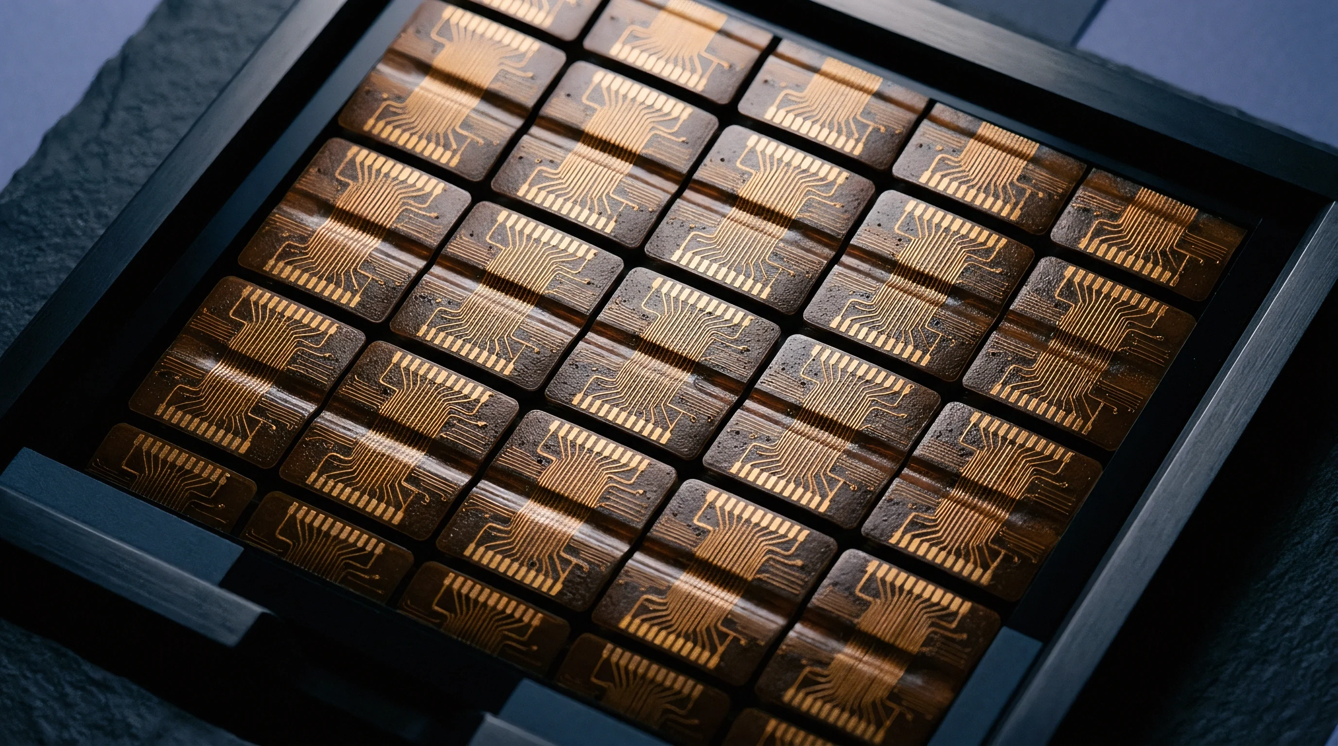
Micro-machined inductive coils and metal-insulator-metal capacitors fabricated on high-resistivity silicon substrates yield sharp stop-band rejection. Integrated Passive Devices (IPD) manufactured on glass or high-resistivity silicon provide Q-factors exceeding fifty at 2 GHz, outperforming standard low-temperature co-fired ceramic (LTCC) embedded passives. Coupling IPD notch networks with SOI switch dies via micro-copper pillar bumps reduces stray interconnect inductances that otherwise shift notch resonance frequencies.
- Resonance Frequency Detuning shifting notch stop-bands away from target harmonic frequencies due to manufacturing tolerances in integrated capacitors and inductors.
- Inductive Substrate Coupling allowing high-power harmonic currents to bypass notch filter networks through parasitic magnetic coupling into adjacent ground planes.
- Thermal Drift Rejection Degradation where elevated module temperature alters dielectric constants, degrading notch rejection by several decibels during sustained transmission.
- Saturation of Passive Components causing non-linear distortion within high-density dielectric layers when subjected to peak RF transmit voltages.
Failing to account for parasitic magnetic cross-coupling between switch inductance loops and module harmonic traps causes certified front end modules to fail final carrier radiated spurious emissions audits.

Verification
Characterizing harmonic distortion on an RF bench demands clean source signals and broad system dynamic range. Standard laboratory signal generators frequently emit second and third harmonic spurs at levels between -40 dBc and -55 dBc when generating output power levels above +10 dBm. Connecting a signal generator directly to a high-linearity RF switch under test results in measuring the source harmonics rather than the switch non-linearity.

Signal Source Spectral Purity Requirements
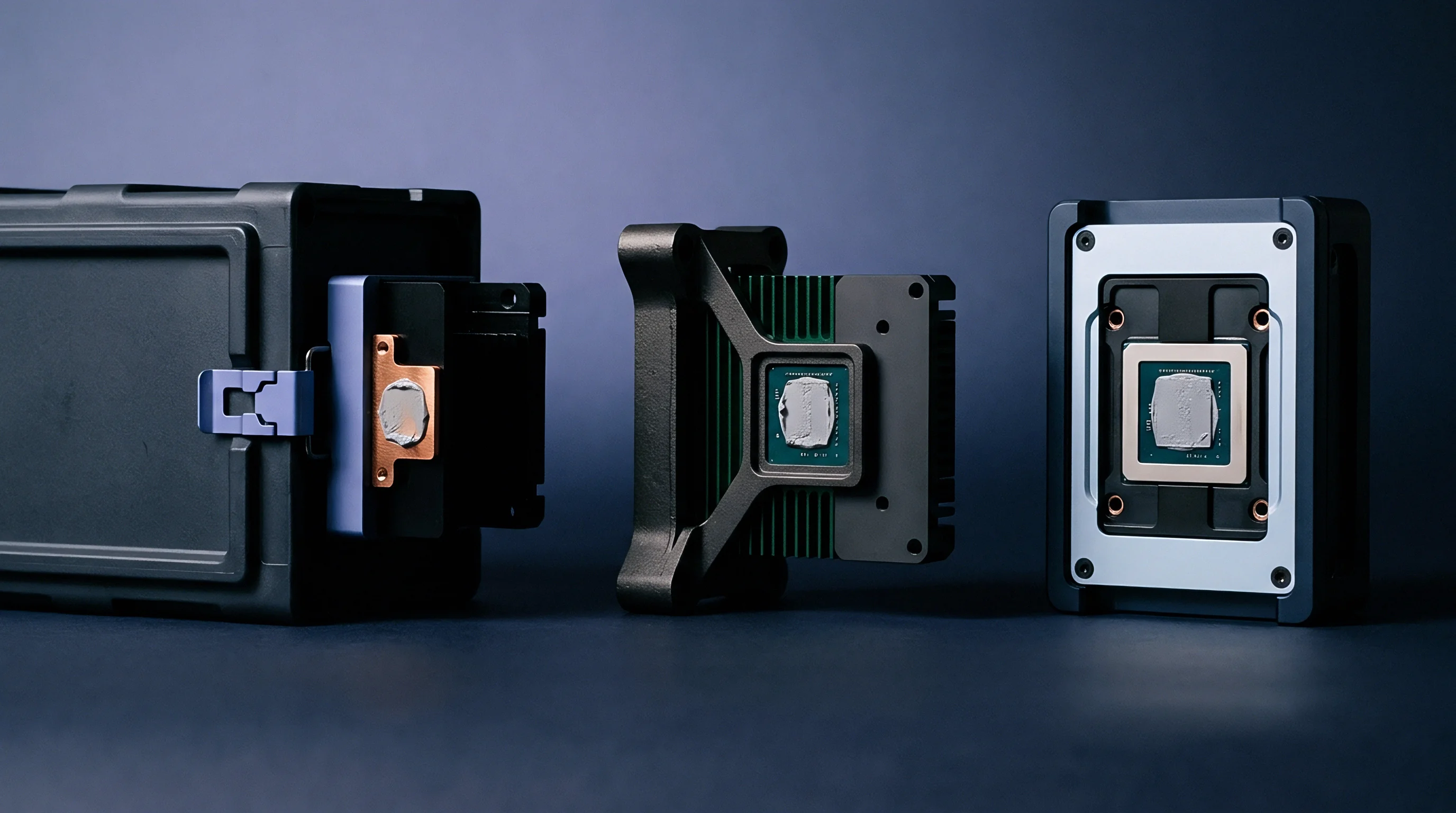
Automated test equipment generators inherently output harmonic distortion that masks switch non-linearity if uncorrected. High-power fundamental signals must pass through high-rejection low-pass clean-up filters before entering the device under test (DUT). A dedicated low-pass filter providing at least fifty decibels of rejection at the second harmonic frequency ensures that the excitation signal arriving at the switch input exhibits harmonic noise levels below -95 dBc.
Coupling path attenuation varies. Spectrum analyzer dynamic range presents a secondary measurement boundary. High-power fundamental signals entering analyzer input mixers generate internal intermodulation and harmonic distortion, creating false measurement readings.
Inserting a high-power fundamental notch filter or tunable band-reject filter between the DUT output and the spectrum analyzer protects the analyzer input mixer from overload while passing high-frequency harmonic signals without attenuation.
Clean drive signals prevent masking. Filter rejection limits switch feedthrough. Verification requires precise power calibration at the switch input pins using a calibrated power sensor to account for cable losses and filter insertion losses across fundamental and harmonic frequencies.
Harmonic level measurements taken without fundamental notch filtering at the spectrum analyzer input reflect internal analyzer mixer distortion rather than switch silicon performance.
Automated Power Sweep and Thermal Drift Measurement
Continuous wave transmit excitation at thirty dBm elevates switch junction temperatures within several hundred milliseconds. Silicon junction heating alters mobility and threshold voltages, causing harmonic generation levels to drift over power pulse durations. Automated bench test routines utilize pulsed RF signals with duty cycles between five percent and ten percent to isolate non-linear junction voltage effects from thermal dissipation effects.
Thermal expansion shifts capacitor values. Comparing pulsed power sweeps against continuous-wave sweeps quantifies thermal drift contributions to third harmonic distortion. Thermal self-heating increases silicon channel resistance, elevating third harmonic generation by two to four decibels during continuous transmit bursts.
- Source Harmonic Floor Audit verifying that clean-up low-pass filter attenuation keeps signal generator harmonics below -95 dBc at the DUT input connector.
- Analyzer Overload Margin Check confirming that fundamental notch attenuation prevents spectrum analyzer internal mixer harmonic generation during high-power drive testing.
- Path Loss Matrix Calibration measuring exact cable, connector, and switch matrix insertion losses across fundamental, second, and third harmonic frequencies using a vector network analyzer.
- Thermal Transient Duty Cycling implementing pulsed RF continuous wave excitation to differentiate voltage-dependent non-linearity from junction thermal degradation.
It remains unclear whether automated production test lines can achieve sub-second test times per switch die while maintaining sufficient dynamic range to measure third harmonics down to -90 dBc under load mismatch.
Compliance
Regulatory bodies and mobile network operators enforce strict limits on spurious radio emissions to prevent spectrum pollution. Global regulatory standards, including FCC Part 15, Part 24, and Part 27 in the United States along with ETSI EN 301 908 in Europe, mandate absolute maximum power limits for radiated spurious emissions. In addition to government regulations, tier-one cellular carriers enforce proprietary approval specifications that dictate substantially stricter harmonic limits.
Regulatory Emission Ceilings and Receiver Desensitization
International standards enforce maximum power spectral density thresholds for all spurious energy generated by mobile transmitters. FCC regulations limit conducted spurious emissions to -13 dBm measured across a 100 kHz or 1 MHz resolution bandwidth, depending on the frequency allocation. Carrier limits exceed generic standards.
Carrier acceptance requirements typically mandate harmonic power levels below -80 dBm or -85 dBm into a matched load, representing a requirement thirty to forty decibels stricter than baseline regulatory floors.
Strict limits protect co-existing radio services. Second harmonic energy from LTE Band 12 (699 MHz – 716 MHz transmit) falls directly into the GPS L1 receive band (1575.42 MHz). If switch harmonic suppression is insufficient, second harmonic leakage bypasses antenna duplexers and desensitizes the co-located GPS receiver, causing position lock failure during active cellular voice or data calls.
Table 3 outlines key regulatory standards and carrier acceptance requirements for cellular front end switches.
| Standard / Specification | Frequency Band | Max Harmonic Level | Measurement Condition |
|---|---|---|---|
| FCC Part 27 Section 53 | AWS / Band 4 | -13.0 dBm EIRP | General Spurious Limit |
| ETSI EN 301 908-1 | Sub-3 GHz Cellular | -30.0 dBm ERP | Conducted / Radiated Floor |
| Tier-1 Carrier Spec A | Low-Band LTE / 5G NR | -85.0 dBm | 2nd Harmonic, 4:1 VSWR |
| Tier-1 Carrier Spec B | Mid-Band LTE / 5G NR | -82.0 dBm | 3rd Harmonic, 1:1 Load |

Sourcing Audits and Lot Acceptance Criteria
Procurement dossiers for cellular modules demand verified test data covering harmonic rejection across production variations. Silicon foundry process shifts, wafer dicing variations, and packaging dielectric tolerances cause batch-to-batch shifts in switch linearity. Sourcing contracts specify lot acceptance sampling rules where sample modules undergo full load-pull harmonic testing before shipment release.
Uncontrollable harmonic variation drives up yield loss at final module test. Sourcing practices specify statistical process control limits on charge pump output voltage and gate bias resistance to guarantee harmonic performance compliance across full production volumes.
Section 4.3 of the Master Cellular Component Supply Agreement mandates that any delivered batch exhibiting second harmonic levels exceeding -80 dBm under a 3:1 VSWR load pull audit triggers immediate rejection of the entire manufacturing lot at the supplier expense.