Micro Coaxial Cable RF Insertion Loss Mechanisms
Micro coaxial cable insertion loss is dominated by conductor skin depth below 3 GHz and dielectric dissipation combined with bend radius distortion above 6 GHz.

Conductor
Signal degradation across sub-millimeter transmission lines originates predominantly within the metallic core and its surrounding outer shield. At radio frequencies, electromagnetic energy does not distribute uniformly across the cross-section of a wire. Current concentrates in a thin outer layer of the metal, driven by counter-electromotive forces induced by internal magnetic flux.
Fine-gauge internal wires in micro-coaxial constructions, ranging from AWG 36 down to AWG 44, possess cross-sectional diameters between 0.127 millimeters and 0.050 millimeters. When operating at frequencies from 2.4 GHz into the sub-6 GHz and 12 GHz bands, this current crowding drastically reduces the effective cross-sectional area available for conduction.
Copper carries high high-frequency current. Silver plating offsets resistive dissipation. Thin wires elevate skin-effect resistance.
The skin depth (δ) defines the depth at which current density drops to 1/e (approximately 37 percent) of its surface value. The relationship depends on resistivity (ρ), operating frequency (f), and magnetic permeability (μ):
δ = sqrtfracρπ f μ
For pure copper at room temperature (20 circC), skin depth equals 1.34 micrometers at 2.4 GHz, shrinks to 0.85 micrometers at 6.0 GHz, and contracts further to 0.60 micrometers at 12.0 GHz. Because an AWG 42 center wire features a physical radius of approximately 31 micrometers, current at 6.0 GHz flows through less than 5 percent of the wire’s total cross-sectional area. The linear resistive component of insertion loss (αc, expressed in dB per meter) increases proportionally with the square root of frequency, governed by the effective surface resistance of the inner and outer metallic structures.
Skin Depth and Current Distribution Mechanics
High-frequency electromagnetic energy travels near the outer boundary of a wire rather than uniformly through its cross-sectional area. Micro-coaxial cables designed for internal radio harness routing prioritize physical flexibility and minimal outer diameter over metallic cross-section. Solid copper inner conductors in fine gauges exhibit poor tensile yield strength, prompting manufacturers to specify silver-plated copper alloy (SPCA) or silver-plated copper-clad steel (SPCCS) cores.
Silver plating provides an outer layer of superior electrical conductivity (σ = 6.30 × 10⁷ S/m) relative to annealed copper (σ = 5.80 × 10⁷ S/m).
| Wire Gauge (AWG) | Nominal Core Diameter (mm) | Core Metallurgy | Skin Depth at 2.4 GHz (μm) | Skin Depth at 6.0 GHz (μm) | Calculated Conductor Loss at 6 GHz (dB/m) |
|---|---|---|---|---|---|
| AWG 36 | 0.127 | Silver-Plated Copper | 1.34 | 0.85 | 1.85 |
| AWG 40 | 0.079 | Silver-Plated Copper | 1.34 | 0.85 | 2.92 |
| AWG 42 | 0.063 | Silver-Plated Copper Alloy | 1.38 | 0.87 | 3.88 |
| AWG 44 | 0.050 | Silver-Plated Copper Alloy | 1.38 | 0.87 | 4.95 |
If the silver plating thickness drops below five skin depths at the lowest operating frequency, RF energy penetrates into the underlying alloy core, elevating attenuation. At 2.4 GHz, five skin depths in pure silver require a plating layer thickness of at least 6.5 micrometers. Commercial micro-coaxial specifications for cost-sensitive Wi-Fi and Bluetooth jumpers frequently restrict silver plating to 1.25 micrometers or 2.5 micrometers.
This thickness constraint forces a portion of the RF current into the higher-resistivity alloy core, adding 0.3 dB to 0.8 dB per meter of unexpected attenuation at lower sub-GHz bands.
At 6 GHz, silver plating of 1.25 micrometers thickness over an AWG 42 center wire maintains attenuation below 4.2 dB per meter at room temperature.
Surface Roughness Factor and Plating Metallurgy
Microscopic peak-to-valley variations along the wire wall force high-frequency currents to traverse an extended physical path length. Inner surfaces alter current flow paths. As skin depth approaches the root-mean-square surface roughness (Rq) of the inner conductor wire, effective resistance rises above classical smooth-wall theoretical models.
The Hemming-Hammerstad surface roughness correction factor (Ksr) quantifies this loss elevation:
Ksr = 1 + frac2π arctan left
For fine wire drawing processes, cold-drawing dies leave longitudinal striations with Rq values between 0.2 micrometers and 0.5 micrometers. At 12 GHz, where skin depth contracts to 0.60 micrometers, an Rq of 0.4 micrometers raises effective conductor resistance by 28 percent over smooth-wire models. The outer return path introduces additional physical complexities.
Micro-coaxial outer shields employ a composite structure containing an inner metal foil wrapped beneath a woven wire braid. Braid coverage percentages below 90 percent leave aperture gaps through which high-frequency magnetic fields escape, elevating effective braid resistance and radiating RF energy into adjacent board circuitry.
- Core Wire Resistivity dictates baseline low-frequency resistance and establishes thermal dissipation limits under high transmit power levels.
- Silver Plating Uniformity prevents localized RF current leakage into high-resistance substrate alloys along cold-drawn wire striations.
- Surface Roughness Profile amplifies high-frequency current path length when profile height exceeds localized skin depth dimensions.
- Braid Coverage Density governs outer conductor surface impedance and shields against electromagnetic coupling into internal system ground planes.
Selecting an ultra-thin cable assembly without verifying the silver plating thickness profile across the center wire risks forfeiting up to 1.5 dB of link margin before environmental thermal derating takes effect.

Substrate
Electromagnetic wave propagation through the insulating layer surrounding the central wire converts radio frequency energy into thermal dissipation. While conductor loss grows with the square root of frequency, dielectric loss increases linearly with frequency. In micro-coaxial designs operating above 5 GHz, dielectric absorption becomes a dominant contributor to overall cable attenuation.
The dielectric loss coefficient (αd, in dB per meter) follows a direct relationship with relative permittivity (varεr), loss tangent (tanδ), and frequency (f):
αd = frac27.3 · f · sqrtvarεr · tanδc
Here c represents the speed of light in vacuum. Heat expands dielectric material volume. Compression shifts outer ground geometry.
Controlling dielectric loss demands insulating materials with both low relative permittivity and exceptionally small dissipation factors across the target temperature range.

Dielectric Dissipation and Frequency Dependence
Energy conversion within non-conducting materials scales linearly with operating frequency, in contrast to resistive losses that grow with square-root relationships. Fluorinated ethylene propylene (FEP), perfluoroalkoxy (PFA), and solid polytetrafluoroethylene (PTFE) serve as standard dielectric substrates in micro-coaxial manufacturing. Solid PTFE features a relative dielectric constant (varεr) of 2.10 and a loss tangent (tanδ) of approximately 0.0002 at 2.4 GHz.
At 6 GHz, dielectric dissipation contributes roughly 0.25 dB per meter in solid PTFE cables. By 15 GHz, this value reaches 0.65 dB per meter, representing a significant percentage of the harness loss budget.
| Dielectric Material | Structure Type | Dielectric Constant (ϵr) | Loss Tangent (tan δ) | Dielectric Loss at 2.4 GHz (dB/m) | Dielectric Loss at 6.0 GHz (dB/m) | Dielectric Loss at 12.0 GHz (dB/m) |
|---|---|---|---|---|---|---|
| Solid PTFE | Dense Polymer | 2.10 | 0.00020 | 0.09 | 0.23 | 0.47 |
| Expanded PTFE (ePTFE) | Porous Micro-Foam | 1.30 | 0.00015 | 0.05 | 0.13 | 0.26 |
| Solid FEP | Melt-Processable | 2.15 | 0.00070 | 0.33 | 0.83 | 1.66 |
| PFA Fluoropolymer | High-Temp Polymer | 2.06 | 0.00030 | 0.14 | 0.35 | 0.70 |
Using lower-cost FEP insulation instead of high-grade PTFE increases dielectric attenuation by more than three hundred percent at 6 GHz due to FEP’s higher loss tangent (tanδ = 0.0007). This difference transforms a functioning link budget into an out-of-spec radio interface during final qualification testing.
Fluoropolymer foam density drops dielectric dissipation while increasing vulnerability to wall collapse during tight chassis routing.
Foam Density and Mechanical Compression
Introducing microscopic air voids into fluoropolymer insulation lowers the effective relative permittivity toward unity. Expanded PTFE (ePTFE) achieves dielectric constants between 1.30 and 1.50 by blowing gas voids into the matrix during extrusion. This structural modification reduces dielectric loss by over forty percent compared to solid PTFE.
It simultaneously accelerates phase velocity from 0.69c up to 0.88c, minimizing phase delays across longer internal jumper runs.
Mechanical vulnerability accompanies this electrical advantage. Micro-foamed structures possess low compressive yield strength. Standard micro-coaxial cable routing inside handheld devices forces assemblies through tight frame channels and around sharp battery bracket corners.
Squeezing a 0.81 mm outer-diameter ePTFE cable reduces the distance between the center wire and outer braid. The characteristic impedance (Z0) drops below the nominal 50-ohm specification, calculated via:
Z0 = frac60sqrtvarεr ln left( fracDd right)
Where D represents the inner diameter of the outer shield and d represents the outer diameter of the center wire. Reducing D through mechanical compression causes localized impedance dips down to 41 ohms, generating severe reflection losses (S11) that compound the elevated dissipation loss of the deformed dielectric wall.
Thinner dielectric walls lower total outer cable diameter but elevate mechanical sensitivity to crush force during housing assembly.
Assembly
Transitions between flexible cable bodies and rigid micro-connectors introduce localized impedance mismatches that compound total transmission loss. A complete cable harness incorporates two connector terminations, typically micro-miniature push-on formats such as u.FL, W.FL, or MHF series (MHF4, MHF5). Reflected power degrades total output gain.
Reflected wave interaction creates voltage standing wave patterns along the cable, converting incident RF power into localized standing waves that elevate dielectric and conductor dissipation at standing wave voltage peaks.
The total system insertion loss (ILtotal) combines smooth-line propagation attenuation (ILline) with input and output reflection losses (ILreflection):
ILreflection = -10 log10 left( 1 – |S11|2 right)
A mated connector pair with a return loss (S11) of -10 dB (VSWR ≈ 1.92:1) incurs a direct reflection loss of 0.46 dB. If both ends of a short 100 mm jumper exhibit -10 dB return loss, multiple internal reflections produce severe attenuation ripple across wideband Wi-Fi 6E/7 channels (5.925 GHz to 7.125 GHz).

Connector Interface Geometry and Discontinuities
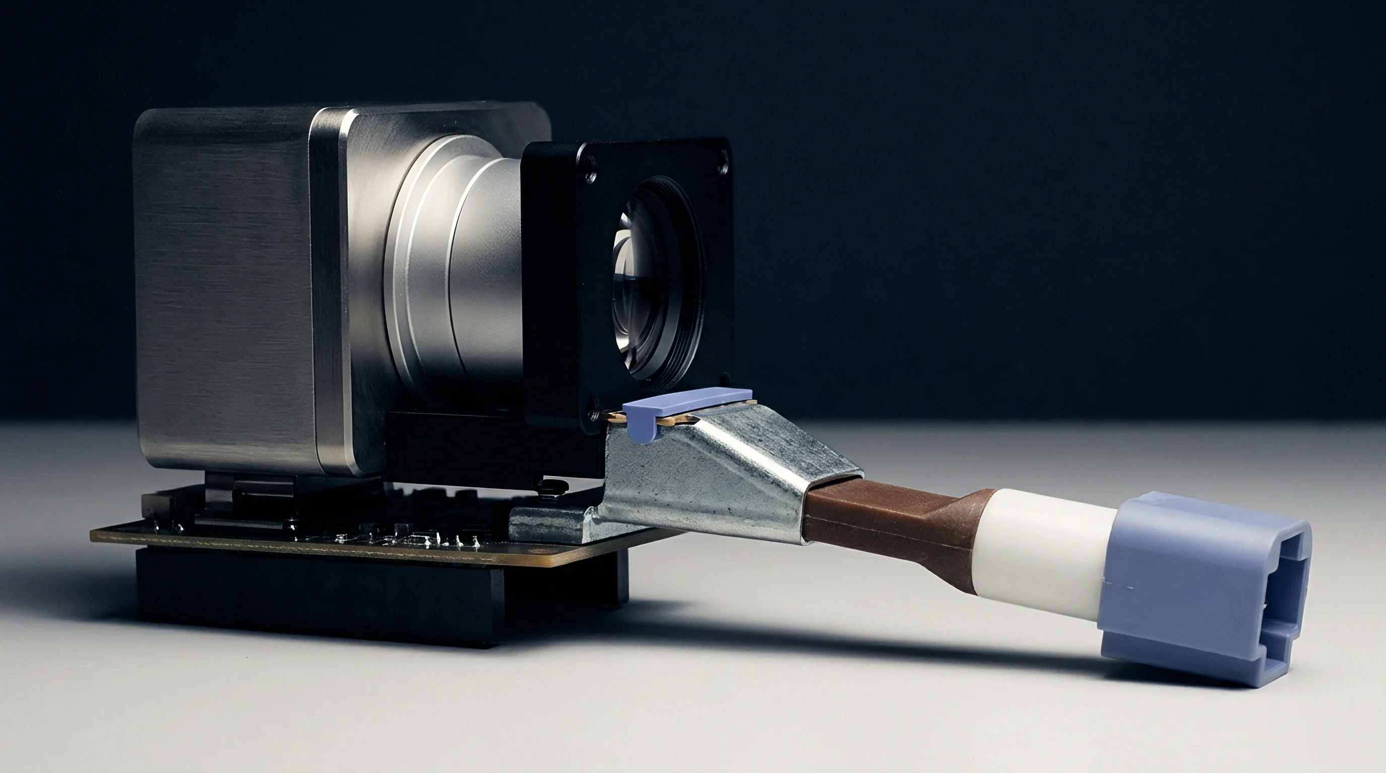
Sub-miniature push-on connectors like u.FL and MHF4 establish mechanical and electrical contact through microscopic pin contacts and outer ground shells. Mated height profiles range from 2.5 mm for standard u.FL down to 1.2 mm for ultra-low-profile MHF4 formats. Shrinking connector physical volume forces structural geometry changes: the internal signal pin diameter drops to 0.15 mm, and dielectric spacing contracts to fractional millimeter dimensions.
Impedance discontinuities inside micro-connector terminations transform return loss spikes into periodic passband ripple across wideband radio transmissions.
Transitioning from a 50-ohm coaxial cable cross-section into a stamped connector socket disrupts the uniform ratio of center conductor diameter to outer shield wall. Stamped ground contacts leave mechanical seam gaps. High-frequency magnetic fields leak through these shell seams, creating localized parasitic inductance (Lstray) and capacitance (Cstray) bumps.
An uncompensated parasitic capacitance spike of 0.15 pF at the solder junction creates a sharp dip in the return loss curve around 5.8 GHz, introducing 0.8 dB of localized insertion loss notch depth.
Solder Wicking and Thermal Termination Defect Modes
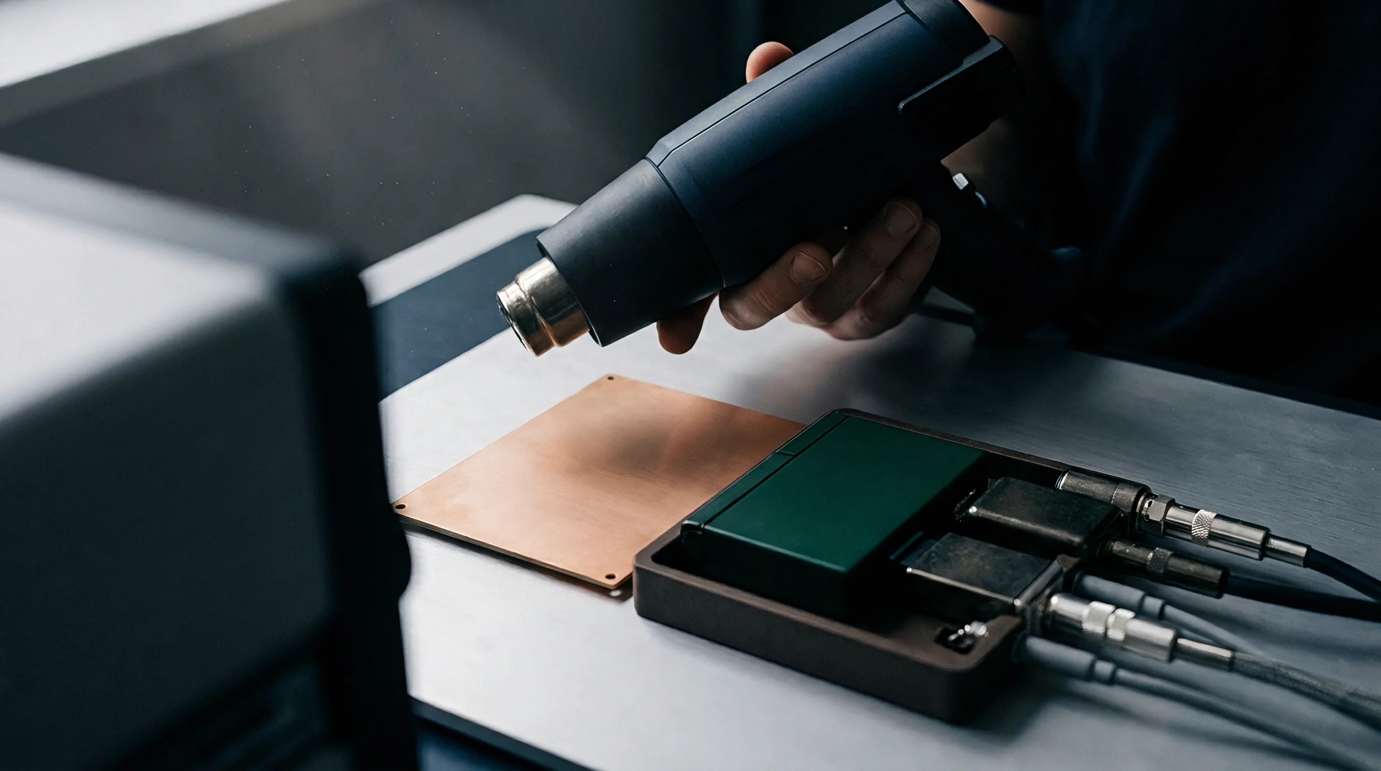
Automated hot-bar soldering of fine center wires to connector pins introduces localized metallurgical changes. Solder wicking alters line impedance. Excess molten tin-lead or lead-free alloy wicks backward along the stranded center core under capillary action, displacing the fluoropolymer dielectric beneath the crimp ferrule.
This liquid metal flow transforms flexible stranded wire into a solid metallic mass while melting the adjacent inner dielectric core wall.
- Solder Bridge Penetration short-circuits internal dielectric space and shifts center conductor concentricity inside the termination ferrule.
- Dielectric Thermal Shrinkback leaves an air gap at the connector interface, creating a low-impedance capacitive discontinuity.
- Ground Shell Crimp Distortion deforms the outer ground barrel, altering spring contact retention force and elevating interface ground resistance.
- Pin Alignment Skew misaligns female socket receivers during mating, causing pin bending and dynamic contact resistance variations under vibration.
Cable suppliers often attribute sudden insertion loss spikes at sub-6 GHz frequencies to customer handling damage during board mounting, masking underlying solder wicking defects generated during factory termination automated processing.
Strain
Physical deformation during chassis installation or dynamic flexing alters the spatial geometry of internal cable elements. Micro-coaxial harnesses routed inside hinged devices, rotating camera gimbals, or tightly packed industrial sensor enclosures experience continuous mechanical stress. Sharp bends distort internal shielding.
Braid separation permits signal leakage. Bending changes the relative positions of center conductor strands, inner dielectric walls, and outer braid wires, inducing physical stress gradients that directly alter high-frequency insertion loss stability.
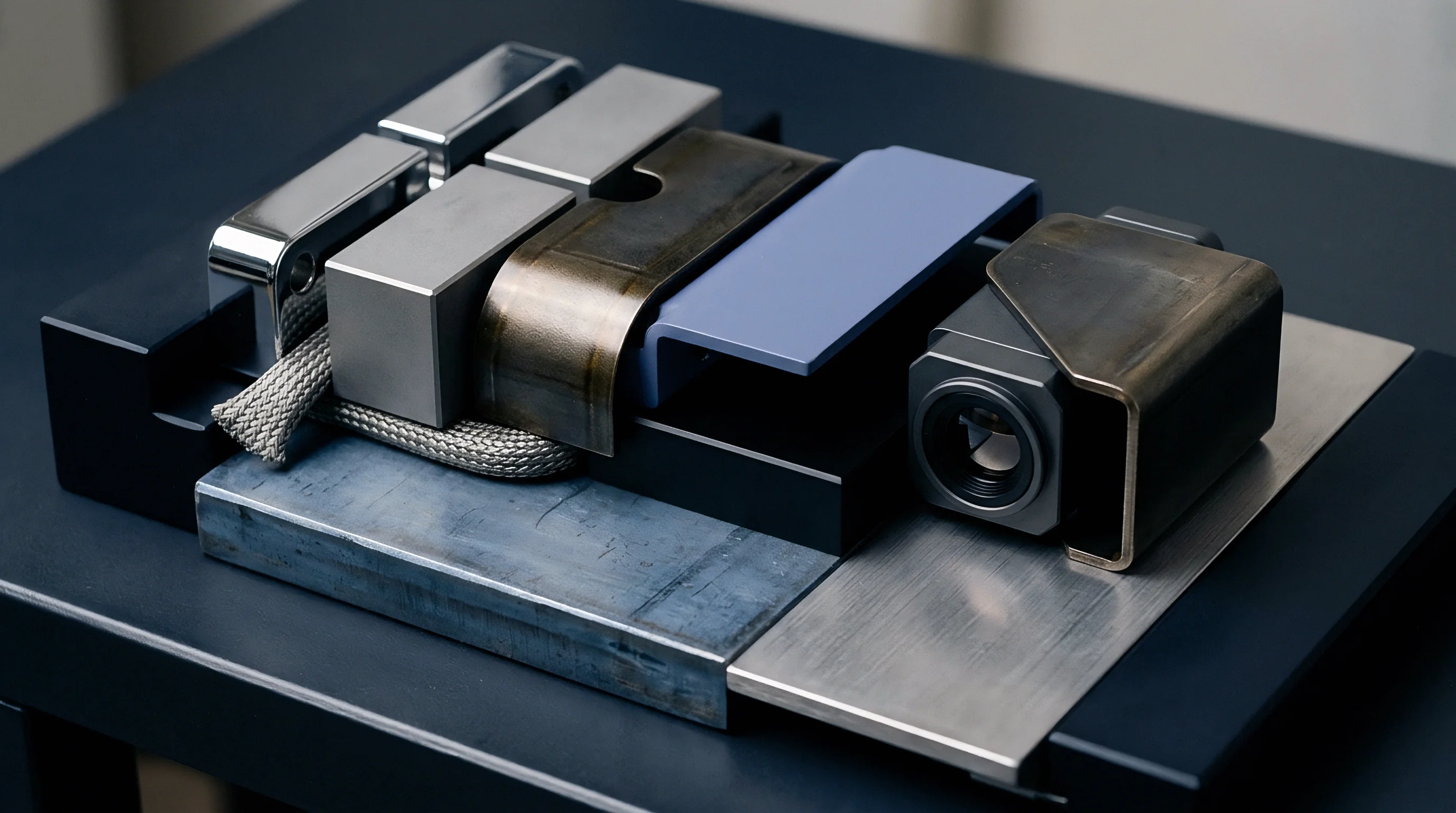
Which Mechanical Deflection Triggers Intermittent Phase Shift?
Bending a flexible micro-coaxial jumper forces the outer braid shield to expand along the outer arc while compressing on the inner radius. This asymmetrical mechanical displacement shifts the center conductor off the central longitudinal axis. Concentricity loss changes the ratio D/d locally around the bend perimeter, altering transmission line impedance and shifting propagation phase velocity.
When the bend radius drops below the manufacturer’s specified minimum threshold, the inner conductor cuts into the soft PTFE or ePTFE dielectric wall.
- Mount the micro-coaxial harness assembly inside an automated two-point mechanical flex fixture with calibrated bend radius mandrels.
- Connect both harness terminations to a vector network analyzer calibrated over the 100 MHz to 12 GHz frequency range using precision adapters.
- Log baseline S-parameters, capturing S21 insertion loss and S11 return loss across the complete operating passband in a relaxed, straight configuration.
- Execute 500 continuous mechanical deflection cycles at a controlled rate of 0.5 Hz while continuously sampling high-speed time-domain transmission metrics.
- Inspect S21 magnitude plots for transient attenuation spikes exceeding 0.3 dB, which signal periodic braid aperture separation during max flexure.
Permanent structural deformation occurs when the bend radius shrinks below four times the overall cable outer diameter (4 × OD). For a 1.13 mm outer-diameter coaxial cable, bending sharper than a 4.5 mm radius causes permanent dielectric wall thinning, shifting baseline attenuation upward by 0.6 dB to 1.2 dB across the 6 GHz to 12 GHz spectrum.
MIL-DTL-17 test procedures mandate insertion loss verification before and after flexural stress cycles to capture shield separation defects.
Shield Separation and Radiation Leakage
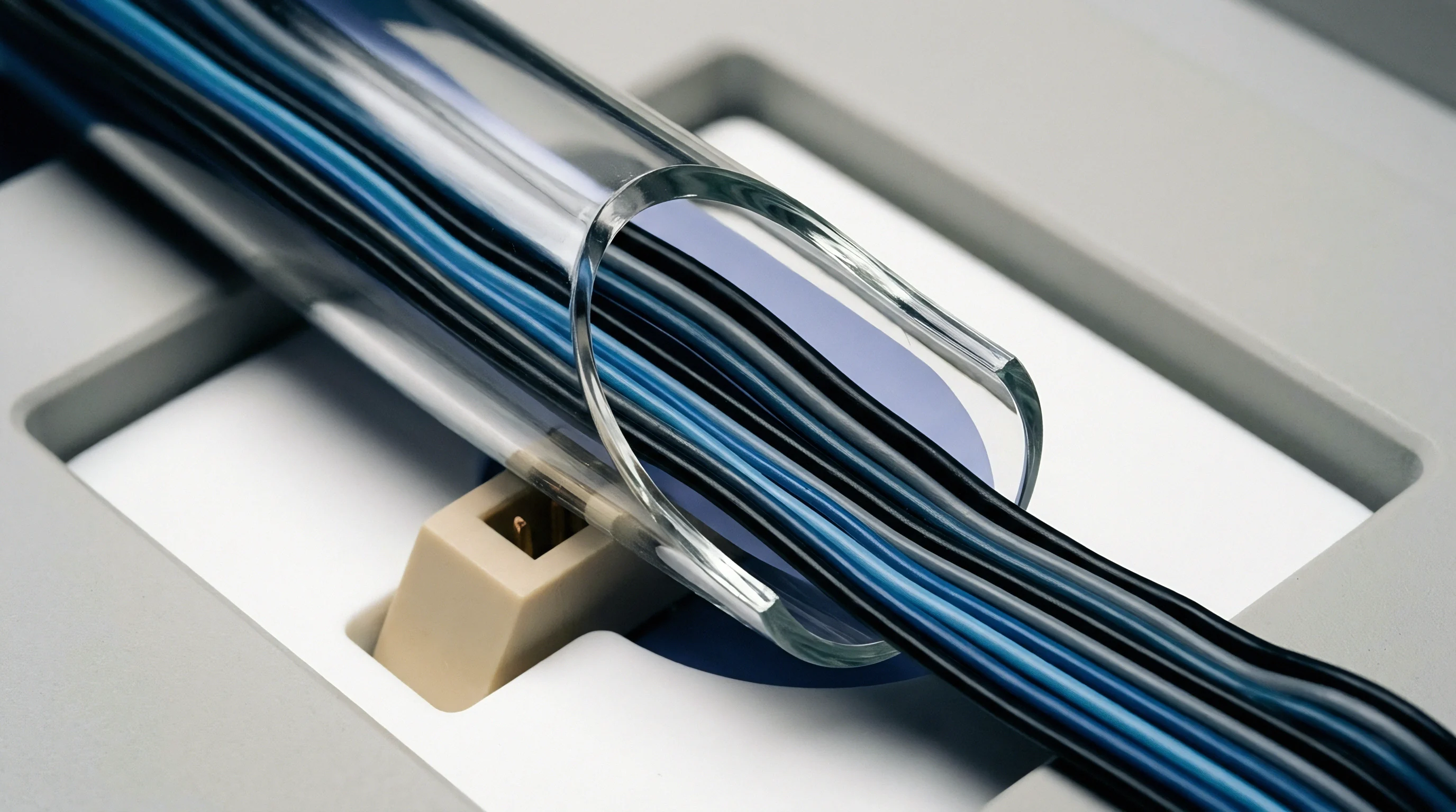
Woven wire braids over metal foils maintain ground integrity under static straight-line conditions. Dynamic flexing opens microscopic gaps between woven braid wire carriers. When braid carrier weave angles shift under mechanical torsion, optical shield coverage drops from a nominal 92 percent down below 75 percent.
High-frequency RF energy escapes through these expanded braid apertures, transforming the micro-coaxial line into a radiating slot structure.
Radiated power leakage directly increases total effective insertion loss. Signal power lost to space through shield gaps subtracts from receiver power at the antenna module port. Furthermore, open braid gaps allow external electromagnetic interference from nearby switching power supplies or digital high-speed lines to couple into the RF path, raising the system noise floor alongside signal attenuation.
Specification compliance documentation must mandate post-flexure RF leakage testing under ASTM D4935 or transfer impedance measurement per IEC 62153-4-3 to guarantee that flex stress does not degrade shield effectiveness below 60 dB at 6 GHz.
Derating
Link budget planning requires adjusting nominal datasheet attenuation numbers to reflect real-world operating environments and fabrication tolerances. Small diameter cables save enclosure space. Margin prevents packet dropping in field deployments.
Environmental thermal cycles shift insertion loss. Standard vendor catalogs quote insertion loss at room temperature (20 circC or 25 circC) under unbent, static laboratory bench conditions. Deploying micro-coaxial jumpers into industrial gateways, automotive telematics units, or outdoor wireless enclosures subjects assemblies to elevated thermal ambient environments ranging from +65 circC to +105 circC.
Temperature Coefficient of Attenuation
Thermal elevation increases metal electrical resistivity while simultaneously altering dielectric loss tangents and physical dimension ratios. Metallic volume resistivity for copper increases at a temperature coefficient (αCu) of approximately +0.393 percent per degree Celsius. As ambient temperature rises from 20 circC to 85 circC (Δ T = 65 circC), center conductor DC resistance increases by 25.5 percent.
Because conductor skin resistance scales with the square root of resistivity, high-frequency conductor loss grows by roughly 12 percent over this thermal delta.
Dielectric absorption increases under high temperatures as polymer chains gain thermal mobility, raising the material loss tangent. Thermal expansion of fluoropolymers also decreases physical density, shifting dielectric constants slightly downward while increasing overall outer diameter dimensions. Combining conductor resistivity elevation and dielectric loss expansion yields an overall temperature coefficient of attenuation (TCA) between +0.15 percent and +0.35 percent per degree Celsius, depending on cable diameter and construction.
| Cable Outer Diameter (mm) | Inner Conductor Gauge (AWG) | Attenuation at 2.4 GHz (dB/m, 20°C) | Attenuation at 6.0 GHz (dB/m, 20°C) | Thermal Loss Elevation at 85°C (dB/m) | Minimum Static Bend Radius (mm) | Estimated Jumper Cost Ratio (150 mm) |
|---|---|---|---|---|---|---|
| 0.81 | AWG 44 | 3.10 | 5.20 | +0.65 | 3.2 | 1.00 |
| 1.13 | AWG 32 | 1.60 | 2.85 | +0.36 | 4.5 | 1.15 |
| 1.37 | AWG 30 | 1.15 | 2.10 | +0.26 | 6.0 | 1.30 |
| 1.78 (Low Loss) | AWG 28 | 0.85 | 1.55 | +0.19 | 8.0 | 1.65 |

Harness Selection Trade-Offs and Link Budget Budgeting
Selecting an interconnect diameter involves balancing insertion loss against mechanical routing constraints inside compact device enclosures. Consider a worked engineering scenario: an IoT gateway housing requires a 150 mm long micro-coaxial jumper connecting an internal M.2 Wi-Fi 6E module to an external SMA bulkhead antenna interface operating at 6.5 GHz. The product operates inside an unventilated outdoor enclosure reaching an internal ambient temperature of +75 circC.
Evaluating an ultra-thin 0.81 mm outer-diameter cable assembly (AWG 44 SPC center wire, solid PTFE dielectric):
Nominal Atteνation at 6.5 GHz (20 circC) = 5.50 dB/m Nominal Cable Loss (0.15 m) = 0.825 dB Connector Pair Mating Loss (2 Interfaces) = 0.350 dB Assembly Room Temp Loss = 0.825 + 0.350 = 1.175 dB
Applying temperature derating for +75 circC operation (Δ T = 55 circC, assuming TCA = +0.25%/ circC):
Thermal Multiplier = 1 + (55 × 0.0025) = 1.1375 Derated Cable Loss = 0.825 × 1.1375 = 0.938 dB
Factoring in a conservative installation bend radius allowance (adding 0.25 dB for mechanical strain distortion near the connector ferrules):
Total Worst-Case Jumper Insertion Loss = 0.938 + 0.350 + 0.250 = 1.538 dB
Link budget audits prevent unexpected field failures. Substituting a 1.37 mm low-loss cable assembly reduces the room-temperature cable attenuation to 2.25 dB/m (0.338 dB for 150 mm). Derated thermal loss drops to 0.384 dB, bringing total worst-case harness insertion loss down to 0.984 dB.
This 0.554 dB margin recovery directly restores lost link budget reach, equivalent to a 13 percent increase in open-field coverage radius for a sensitivity-limited radio receiver.
Procurement documentation for high-reliability RF jumpers must mandate comprehensive submission dossier packages containing batch trace data.
- Batch Plating Thickness Verification reports confirm silver plating depth across inner core wire lots via X-ray fluorescence measurement.
- Swept High-Frequency S-Parameter Trace Data validates attenuation and return loss compliance across the complete 100 MHz to 12 GHz band.
- Thermal Cycling Verification Dossiers certify insertion loss drift stays within specification limits across -40 circC to +85 circC thermal shock profiles.
- Flexural Endurance Test Certificates prove assembly stability under continuous deflection cycles without mechanical braid degradation.
What long-term degradation mechanics govern the attenuation stability of micro-foamed dielectric micro-coax harnesses when exposed to sustained industrial vibration combined with high atmospheric humidity?