Sub-GHz Radio Power Transients during SPI Flash Page Program Interrupts
Mitigate sub-GHz radio power transients during flash page writes using split supply rails, DC-bias derated capacitors, and firmware program-suspend arbitration.

Rail
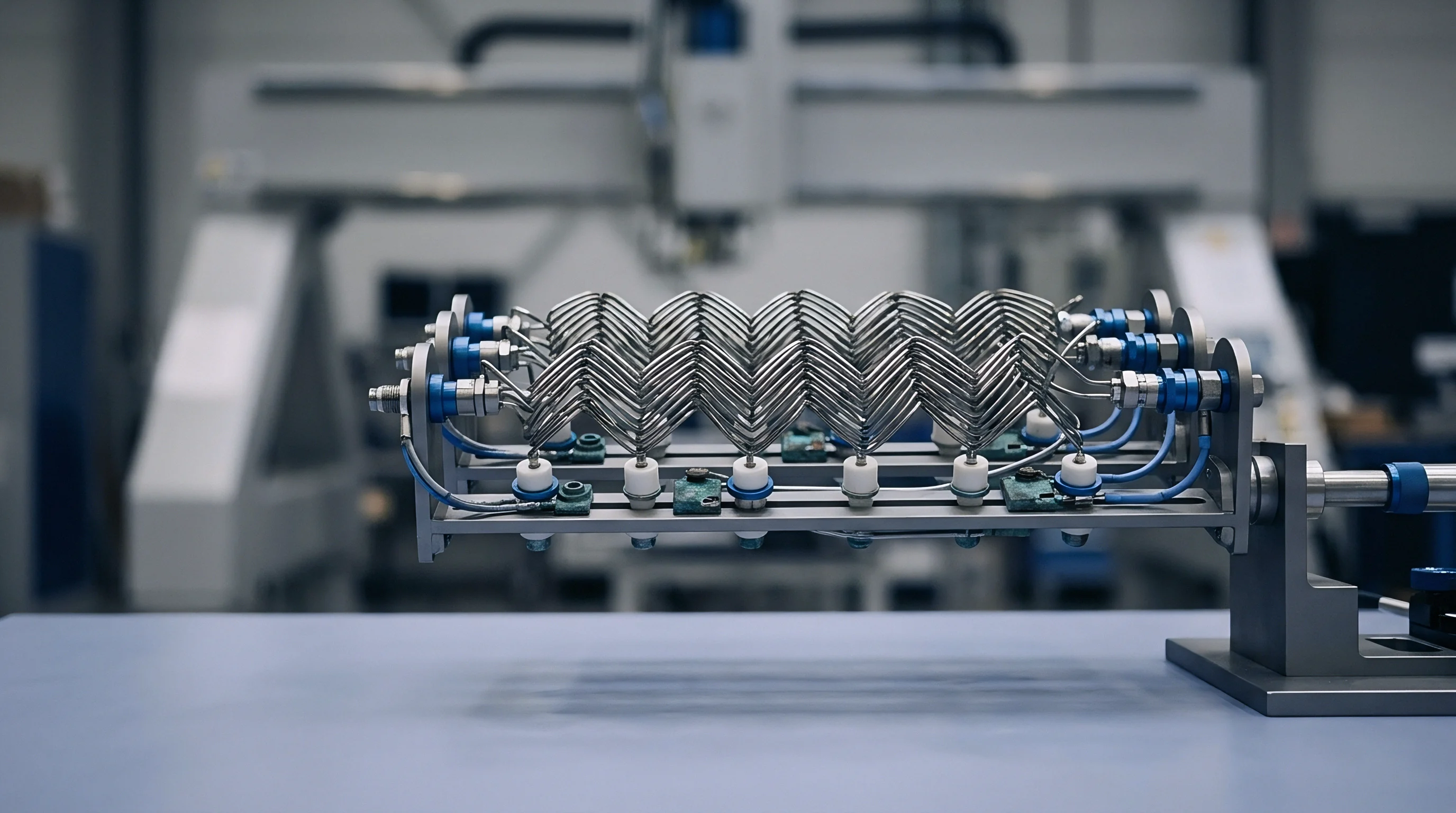
Current probes placed at the feed point of an integrated transceiver reveal steep supply drops when the transmitter ramps up while external nonvolatile memory is drawing write current. A sub-GHz transmission burst delivers +14 dBm to +22 dBm into an antenna matching circuit. At +22 dBm output, power amplifier drain current climbs from tens of microamperes in sleep to 120 milliamperes within 12 microseconds.
If an asynchronous interrupt demands radio transmission while an SPI NOR device is running internal charge pumps to erase or write a page, the sudden combined load pulls the primary supply down with a slew rate exceeding 0.8 volts per microsecond. Lithium thionyl chloride cells and depleted alkaline packs exhibit internal resistance ranging from 15 ohms to 40 ohms at sub-zero temperatures. That source resistance converts a 135 milliampere combined pulse into an instantaneous drop exceeding 2.0 volts, driving the digital supply well below the operating limits of memory chips and baseband processors.
A 35-ohm cell impedance exposed to a 130-milliampere combined load drops the supply by 4.55 volts, which forces immediate hardware shutdown on a 3.3-volt nominal bus.
Brownout Thresholds and Battery Source Impedance
Microcontrollers monitor supply rails through internal analog comparators tied to fixed trip points. Standard factory configurations set brownout reset triggers at 2.1 volts, 2.4 volts, or 2.7 volts. A 3.0-volt coin cell powering a remote sensor holds nominal voltage during quiescent periods.
When transceiver activation coincides with flash bit manipulation, equivalent series resistance drops the delivered bus voltage below the programmed 2.1-volt boundary within six microseconds. The comparator trips reset logic immediately, cutting off CPU execution mid-instruction. The external SPI chip remains in an active high-voltage programming state while its serial clock line floats or transitions unexpectedly, freezing peripheral state machines.
Reset loops become self-sustaining when firmware re-enters radio transmission directly upon boot before the battery has had time to recover open-circuit charge.

Simultaneous Conduction during Memory Write Cycles
Energy delivery networks face compounded current draws when peripheral devices share a single low-dropout linear regulator or buck converter. The baseline radio transmission requires heavy current, while external SPI memory pulls a continuous base current superimposed with microsecond-scale spikes from its internal voltage multiplier. Typical failure behaviors emerge when the energy delivery circuit fails to maintain supply integrity:
- Brownout Reset Assertion drops the main processing unit into hardware reset, cutting off control communication while external memory charge pumps continue discharging into the substrate.
- Write Enable Latch Corruption flips internal register logic when voltage collapses below the minimum write inhibit specification, leaving memory arrays vulnerable to invalid partial writes.
- Radio Phase Lock Disruption pulls the transceiver supply below the local oscillator phase-locked loop charge-pump headroom, which degrades the spectral mask and generates out-of-band spurious emissions.
- Flash High Voltage Collapse cuts program voltage inside the memory matrix, freezing electron tunneling and resulting in half-programmed cells with indeterminate logic levels.
Designs neglecting source impedance during combined transient events suffer silent flash block corruption and persistent operational lockout across field deployments.


Surge
Antenna drivers operating in the 868 MHz and 915 MHz allocations demand extreme current transitions across short rise envelopes. A Class-E power amplifier driving +22 dBm requires rapid collector or drain bias charging, drawing up to 140 milliamperes at 3.3 volts. Regulatory specifications govern RF spectral roll-off, requiring transmitter power amplification to ramp up over precisely shaped curves between 2 and 32 microseconds.
Short ramp durations minimize packet overhead and preserve transmission airtime allocations under regional band rules. Fast ramping generates high di/dt conditions across supply pin wirebonds, decoupling loop inductances, and printed traces, producing inductive voltage kicks across decoupling nodes.

Sub-GHz Power Amplifier Turn-On Dynamics
Direct modulation architectures apply bias voltage across pre-driver and output stages along calibrated ramps to prevent adjacent channel splatter. Power amplifier drain current tracks output wattage non-linearly. A +14 dBm transmit step pulls 45 milliamperes through the radio terminal, whereas a +20 dBm setting demands 85 milliamperes, and +22 dBm exceeds 120 milliamperes.
The table below compiles current consumption figures, ramp timings, and transient rail deflections measured across representative sub-GHz transceivers operating from an unregulated 3.0-volt source with 5 ohms internal resistance.
| Transceiver Family | Frequency Band | Output Power | Ramp Duration | Peak Current | Maximum Rail Deflection |
|---|---|---|---|---|---|
| Integrated SoC Sub-GHz | 868 MHz (Europe) | +14 dBm | 10 µs | 46 mA | 230 mV |
| Discrete High-Power Transceiver | 915 MHz (Americas) | +20 dBm | 8 µs | 88 mA | 440 mV |
| Long-Range Proprietary RF IC | 868 MHz (Europe) | +22 dBm | 4 µs | 124 mA | 620 mV |
| Multi-Band Ultra-Low Power IC | 915 MHz (Americas) | +14 dBm | 16 µs | 38 mA | 190 mV |
| High-Output Telemetry Chipset | 923 MHz (Asia) | +22 dBm | 2 µs | 136 mA | 680 mV |
Transient voltage drops track power amplifier output ratings directly and scale inversely with ramp duration. Rapid ramps impose steep current demand steps. Slower ramps smooth power distribution, preserving rail stability at the expense of higher packet energy consumption.

Harmonic Trap Resonance and Inrush Magnitude
Printed matching circuits interpose discrete inductors, capacitors, and printed transmission lines between the transceiver output pin and the antenna connector. A high-efficiency differential-to-single-ended balun combines with a multi-pole low-pass filter to attenuate the second and third harmonics. When the power amplifier transitions from tri-state to saturation, reactive filter components pull inrush displacement current to establish field potentials.
Resonance rings at the tank frequency before stabilizing into steady-state sinusoidal conduction. The resulting high-frequency ringing superimposes upon the primary supply transient, generating radio frequency ripple voltages exceeding 150 millivolts peak-to-peak that propagate along the board layout to adjacent digital components.
- Verify that the primary DC supply track isolates the RF power amplifier feed from the memory VDD pin through a high-frequency ferrite choke.
- Implement soft-start transmitter ramping in firmware registers to expand the power amplifier power-up envelope from 2 microseconds to 16 microseconds.
- Insert a series decoupling resistance of 1 to 2 ohms on the memory supply input to decouple fast transient resonance loops from the SPI bus pins.
- Configure peripheral input-output driver slew rate registers on the memory interface to slow transition speeds down to 50 nanoseconds.
Transient sag below published absolute ratings is routinely documented as harmless provided the duration stays under 50 nanoseconds, yet in-circuit testing reveals sector data losses under precisely those brief dips.

Flash
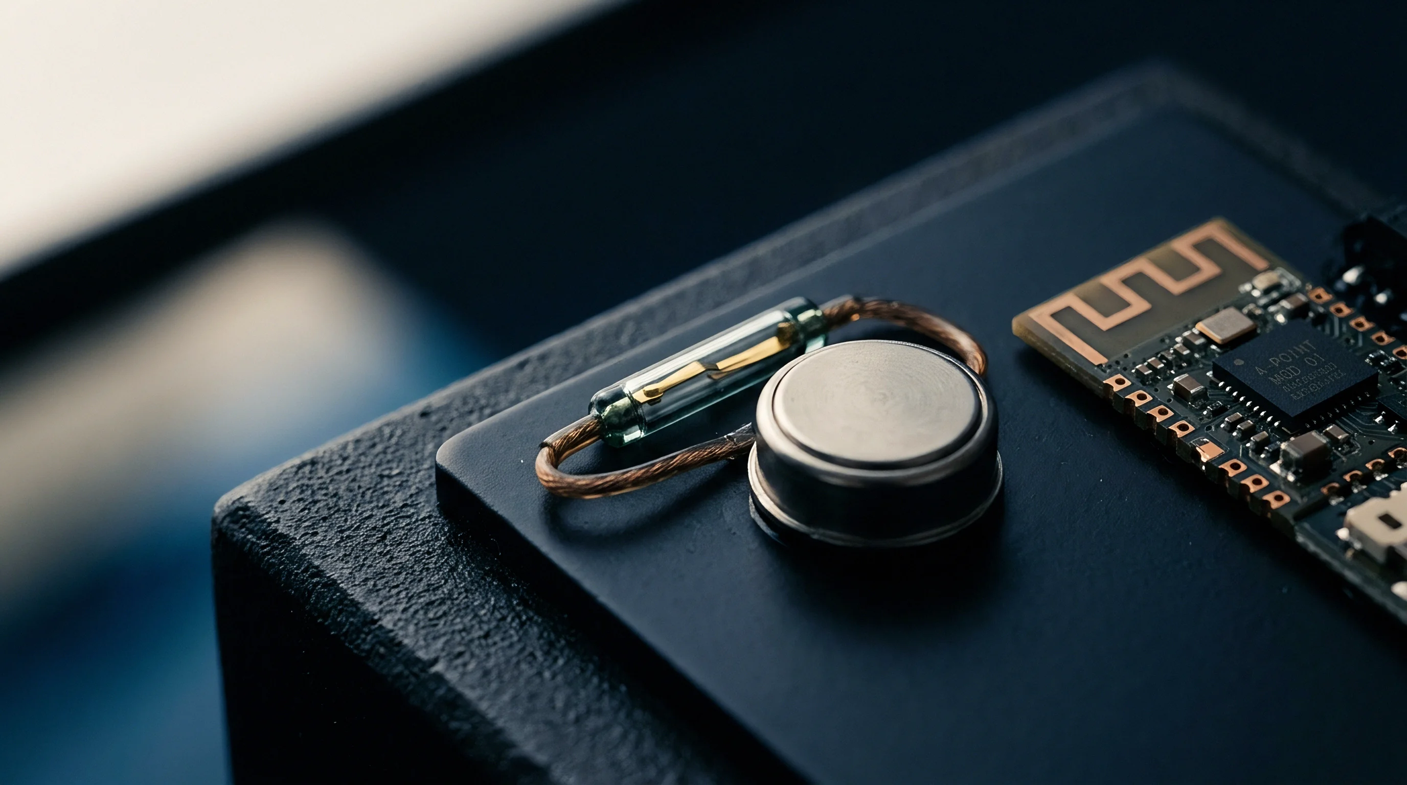
Semiconductor nonvolatile storage devices utilizing serial peripheral interface connections employ internal charge pump matrices to write floating-gate or charge-trap memory cells. Programming a single page requires moving 256 bytes into internal SRAM latches, followed by the activation of high-voltage switches applying 10 to 12 volts across target dielectric gates. This high-voltage cycle lasts between 0.4 milliseconds and 3.0 milliseconds depending on die generation and wear history.
The charge pump draws an active programming current of 5 to 15 milliamperes from the VDD pin in pulsed bursts that coincide with internal oscillator cycles. These bursts generate internal current steps at frequencies between 10 MHz and 50 MHz, modulating the base current demand.
Under section 4.2 of JEDEC Standard 216D, nonvolatile devices must maintain valid data retention when VDD remains strictly within operating limits throughout the page program cycle.

Page Program Charge Pump Physics
Electron tunneling across thin oxide layers requires unyielding electrostatic fields. If VDD collapses while high voltage acts across an array sector, electron transit stalls midway through the program threshold band. The memory cell is left in an indeterminate marginal state where sensory amplifiers read it as erased or programmed depending on die temperature and supply variation.
A read margin collapse causes cyclic redundancy check failures during subsequent boot scans. Erasing or reprogramming corrupted pages requires entire block erase cycles, accelerating silicon wear. The following dataset documents program times, suspend latencies, and write inhibit thresholds across commonly sourced 64-megabit SPI NOR flash devices.
| Device Manufacturer Tier | Operating VDD Range | Page Program Time (Typ) | Program Current (Max) | Program Suspend Latency | Write Inhibit Voltage |
|---|---|---|---|---|---|
| Industrial Tier A (Winbond W25Q64JV) | 2.7 V to 3.6 V | 0.7 ms | 15 mA | 20 µs | 2.25 V |
| Industrial Tier B (Macronix MX25L6433F) | 2.7 V to 3.6 V | 0.8 ms | 12 mA | 25 µs | 2.40 V |
| Ultra-Low-Power Tier (Adesto AT25SL641) | 1.7 V to 3.6 V | 1.5 ms | 6 mA | 35 µs | 1.55 V |
| Automotive Tier (Micron MT25QL064) | 2.7 V to 3.6 V | 0.4 ms | 18 mA | 30 µs | 2.30 V |
Suspending a write sequence requires issuance of the command byte 75h via the SPI bus. The memory controller pauses internal pumping, discharges high-voltage nodes through pull-down paths, and sets the suspend status flag in its internal read register. This discharge sequence consumes significant airtime budget.
Latencies vary between 20 and 40 microseconds across suppliers. If a high-priority sub-GHz radio transmission occurs before the suspend process fully drains the pump circuitry, the supply bus experiences peak radio current while the storage IC still draws charging current. The overlapping drain drives the bus voltage below the write inhibit voltage, corrupting data in transit.

Can Program Suspend Mask RF Slew Faults?
Executing an interrupt service routine to suspend nonvolatile programming before initiating radio packet transmission prevents direct current overlap. The processor traps the inbound radio event, asserts the chip select line, clocks out the 75h suspend opcode, and loops on reading status register 2 until the suspend bit toggles. While logical overlap disappears, physical supply transients persist.
Suspending the memory load induces an abrupt reduction in supply draw, producing an inductive flyback spike on the rail. When the radio power amplifier turns on immediately afterward, the rail snaps downward. The resulting voltage swing stresses output stage decoupling networks, perturbing phase noise on local oscillators and triggering peripheral bus timeouts.
Engineers evaluate whether dynamic firmware delays or autonomous hardware interlocks deliver superior protection against unpredictable cell degradation over multi-year deployment periods.

Decoupling
Energy storage placed directly at the pin delivers current during sudden step loads, catching the rail before the primary regulator loop can react. Multi-layer ceramic capacitors serve as the primary defensive barrier. Standard layouts specify 10-microfarad or 22-microfarad capacitors in 0402 or 0603 footprints on the assumption that rated capacitance is available during load transitions.
Ceramic dielectrics lose substantial capacitance when direct-current operating voltages approach package limits. An X5R or X7R capacitor rated at 6.3 volts loses 40 to 60 percent of its nominal capacitance when biased at 3.3 volts. In an 0402 package, a nominal 10-microfarad capacitor yields only 3.8 microfarads in normal circuit conditions.
Calculations based on nominal values alone fail to arrest high di/dt rail drops because they ignore this direct-current bias derating.
A ceramic capacitor subjected to continuous direct-current operating voltage near its rated limit forfeits more than half its nominal storage capacity before transient events begin.

Capacitance Loss under Direct-Current Voltage Bias
Ferroelectric domain pinning within high-permittivity ceramic layers restricts dipole realignment under continuous electric fields. As direct-current bias increases, permittivity falls, reducing usable capacitance. Package scale governs this degradation.
A 10-microfarad capacitor in an 0805 case retains higher capacitance than the identical rating inside an 0402 case under an identical 3.3-volt bias. The table below illustrates direct-current bias degradation across multi-layer ceramic capacitors commonly placed adjacent to sub-GHz radio transceivers and SPI memory components.
| Case Footprint | Dielectric Type | Nominal Value | Rated Voltage | Effective Capacitance (3.3V) | Total Rail Drop (120mA / 10µs) |
|---|---|---|---|---|---|
| 0402 (1005 Metric) | X5R | 10 µF | 6.3 V | 3.6 µF | 333 mV |
| 0603 (1608 Metric) | X7R | 10 µF | 10 V | 6.8 µF | 176 mV |
| 0603 (1608 Metric) | X7R | 22 µF | 6.3 V | 9.2 µF | 130 mV |
| 0805 (2012 Metric) | X7R | 22 µF | 16 V | 16.5 µF | 72 mV |
| 0805 (2012 Metric) | X7T | 47 µF | 6.3 V | 24.8 µF | 48 mV |
Transient voltage drop scales in inverse proportion to effective capacitance. Deploying 0402 capacitors compromises supply rail integrity during concurrent peripheral operation. Moving to 0603 or 0805 cases with higher voltage ratings preserves charge storage, attenuating voltage deflections during heavy current transients.

Low-Dropout Regulator Step-Load Recovery Benchmarks
Active regulators exhibit closed-loop recovery bands ranging from 5 to 50 microseconds. When a radio transmission starts, the output pass transistor remains in its prior conduction state until the error amplifier detects a voltage drop across its feedback network. During this response latency, load current flows exclusively from local decoupling capacitors.
If the decoupling network drains before the regulator feedback loop increases current delivery, the rail continues its descent. When the error amplifier responds, the output transistor snaps open, causing rail overshoot. This overshoot generates high-frequency voltage spikes across the SPI flash, exceeding maximum operating ratings and creating latch-up risks.
A well-proportioned decoupling network places its lowest resonant impedance directly at the transient frequency of the radio power amplifier ramp.


Arbitration
Hardware isolation separates high-priority sub-GHz radio transactions from concurrent nonvolatile memory programming. When sensors detect alarm conditions, radio transmission cannot endure millisecond-scale pauses without risking channel contention, telemetry dropouts, or protocol state machine failures. Hardware architectures incorporate split supply lines using dedicated low-dropout regulators for radio and memory stages.
A processor controls an analog switch or load gate that isolates memory power during emergency radio operations. Firmware schedulers govern transmission intervals using state machines that prohibit parallel peripheral operations.

Firmware Event Scheduling and Hardware Sockets
Firmware architecture establishes structural protection against concurrent power draws. Real-time scheduling prevents memory write routines from executing during active or pending radio windows. The operating system handles radio interrupts by signaling memory tasks through an event semaphore.
Memory tasks pause page write commands until clear channel assessment and packet transmission routines finalize. The decision matrix below establishes operational boundaries for peripheral activity based on battery state and radio priority levels:
- Critical Telemetry Frames preempt all memory operations, commanding immediate page write suspension or peripheral power gating to preserve maximum RF power amplifier output.
- Periodic Sensor Logging postpones radio activation until the active memory page program sequence clears the internal charge pump cycle.
- Low-Battery States mandate reduction of radio output power from +22 dBm to +14 dBm, constraining peak current within battery internal resistance limits.
- Firmware Over-The-Air Updates restrict memory writes to quiescent radio reception intervals, disallowing simultaneous flash page programming during packet acknowledgement transmissions.
Dividing peripherals across independent supply domains resolves current contention. A dedicated radio regulator isolates transmitter inrush spikes, protecting digital storage buses from rail collapse.

Regulatory Airtime Limits and Commercial Liability
Regional spectrum regulations place constraints on transmission behavior across license-free sub-GHz bands. In the European Union, ETSI EN 300 220-2 imposes strict duty cycle ceilings: 0.1 percent, 1.0 percent, or 10 percent depending on sub-band allocation. Devices exceeding these airtime ceilings risk regulatory fines, customs confiscation, and product recalls across target territories.
In North America, FCC Part 15.247 allows continuous transmissions if spread-spectrum hopping or digital modulation parameters comply with spectral density constraints. Suspending memory operations to prioritize immediate radio transmission introduces packet jitter, altering transmission cadences. Sourcing organizations include verified power-rail transient stability clauses within hardware delivery agreements, obligating silicon and module suppliers to cover warranty and recall expenses if rail-collapse corruption corrupts devices in the field.
Standard delivery contracts enforce compliance through Section 8.4 of the IPC-A-610 qualification terms, making suppliers liable for replacement costs when field failures stem from inadequate power rail decoupling.