Surface Roughness Impact on Radio Frequency Contact Impedance
Surface roughness elevates RF contact impedance by shrinking real metal contact area and forcing current paths over microscopic peaks exceeding skin depth.

Skin
At radio frequencies, alternating current does not distribute uniformly through a conductor’s cross-section. Internal magnetic flux forces charge density toward the outer skin of a trace, wire, or contact, restricting effective conduction to a thin surface layer that shrinks inversely with the square root of frequency and magnetic permeability.
At sub-GHz frequencies like 868 MHz or 915 MHz, the skin depth in copper is roughly 2.2 micrometers. In the 2.4 GHz band used by Bluetooth Low Energy and Wi-Fi, that conduction depth narrows to 1.3 micrometers. By the time signals reach sub-6 GHz cellular bands or 24 GHz to 77 GHz millimeter-wave radar and satellite backhaul, skin depth drops below 400 nanometers ~ a scale where surface topography no longer acts like a smooth plane.
Electromagnetic Current Distribution at Conductive Boundaries
Surface losses compound as frequency rises. When peak-to-valley profile heights approach or exceed the penetration depth, propagating wavefronts trace the physical contours of the metal rather than traveling in a straight axial path. These microscopic contours force current along longer physical routes, raising the effective phase constant and AC resistance well above theoretical bulk values.
Topographical variations distort the magnetic field surrounding the conductor boundary. Current crowding around sharp micro-peaks creates localized hotspots and parasitic inductance. Smooth rolled copper foils keep root-mean-square roughness below 300 nanometers, preserving predictable insertion loss across microstrip transitions.
By contrast, reverse-treated or electrodeposited coppers can exhibit peak-to-valley profiles over 3 micrometers, driving insertion loss up by 30 to 110 percent across the 10 GHz to 60 GHz spectrum.
| Frequency Band | Operating Frequency | Theoretical Skin Depth (µm) | Threshold Surface Roughness Rq (µm) | Attributed Attenuation Increase (%) |
|---|---|---|---|---|
| Sub-GHz IoT | 915 MHz | 2.16 | > 2.20 | 4 to 8 | 2.4 GHz ISM | 2.45 GHz | 1.32 | > 1.30 | 12 to 18 | 5 GHz Wi-Fi | 5.80 GHz | 0.86 | > 0.80 | 25 to 35 | Sub-6 GHz Cellular | 3.50 GHz | 1.11 | > 1.10 | 15 to 22 | mmWave Radar | 24.125 GHz | 0.42 | > 0.35 | 45 to 75 | mmWave Backhaul | 60.00 GHz | 0.27 | > 0.20 | 80 to 140 |
Modeling Attenuation from Sub-GHz to Millimeter Bands
Classical models such as the Hammerstad-Jensen equation adjust for root-mean-square surface roughness by scaling attenuation according to idealized hemispherical or triangular profiles. While reliable below 10 GHz, Hammerstad formulations underestimate losses at higher frequencies because they model the boundary as a continuous wave path instead of an array of three-dimensional scattering shapes.
Modern board-level verification relies heavily on the Huray gradient model, which represents the substrate-copper interface as base-mounted spherical nodules. By calculating the ratio of total sphere surface area to flat base area, Huray accounts for actual spatial current redistribution over electrodeposited copper. When specifying PCB stackups for high-frequency radio modules, matching substrate roughness to the target wavelength prevents link budget degradation before silicon is even placed.
Designing RF interfaces requires maintaining surface profile heights well below the skin depth of the highest operational harmonic.


Asperity
Solid metal surfaces are never flat at the microscopic scale. When two conductors mate inside an RF connector, pogo pin joint, or test socket, contact occurs only at high points known as asperities. Under typical mechanical clamping force, the actual contact area is often less than one percent of the apparent geometric area.
Current flow compresses through these narrow touchpoints, producing constricted conduction paths. This constriction increases contact resistance, while the uncontacted valley voids act as microscopic parallel capacitors and series inductors that distort local characteristic impedance.
When Can Mechanical Surface Polishing Reduce Millimeter Wave Feed Losses?
Mechanical polishing reshapes the contact interface by leveling microscopic peaks to increase real contact area. At frequencies above 10 GHz, dropping profile roughness from Ra 1.6 micrometers to Ra 0.2 micrometers reduces localized RF contact impedance variance from 8.5 ohms to under 0.4 ohms across the mating boundary.
Polishing also removes air voids that create parasitic dielectric discontinuities. Trapped air carries a relative permittivity of 1.0, compared to values between 2.2 and 4.3 for the surrounding substrate or connector dielectric. This permittivity step creates localized impedance drops, reflecting RF energy back toward the power amplifier and degrading total radiated power.
At 24 GHz, a contact interface compressed under 5 Newtons of force with an average roughness of 1.2 micrometers exhibits a 1.4 dB higher insertion loss than the same contact finished to 0.2 micrometers.

Deformation Dynamics under Mechanical Contact Pressure
Mechanical force governs micro-scale behavior at the contact interface. Initial clamping elastically deforms the tallest peaks. As force increases, local pressure exceeds the yield strength of the surface plating, inducing plastic deformation that flattens asperities and widens contact spots.
Plastic deformation lowers RF contact resistance by establishing direct metal-to-metal bonds across clean micro-junctions. Without enough clamping force, the interface remains in an elastic regime where vibration or thermal cycling constantly shifts the contact area, modulating interface impedance and introducing amplitude modulation noise into transmitted signals.
Mechanical retention designs must supply sufficient mating force to transition microscopic contact points from elastic deflection into stable plastic deformation.
- Asperity Constriction Resistance increases DC and AC power loss at the mating plane as current paths narrow through microscopic metallic touchpoints.
- Parasitic Air Cavity Reactance introduces localized reactive impedance drops, creating mismatches along microstrip feeds and raising voltage standing wave ratios.
- Fretting Wear Debris collects in surface valleys during vibration, forming semi-conductive oxide layers that elevate contact noise.
- Non-Uniform Current Distribution concentrates RF current into localized hotspots, driving thermal cycles that weaken mechanical retention spring force over time.
Specifying mechanical spring force without tightly controlling mating surface roughness leads to field failures when contact resistance drifts out of specification under environmental stress.

Joint
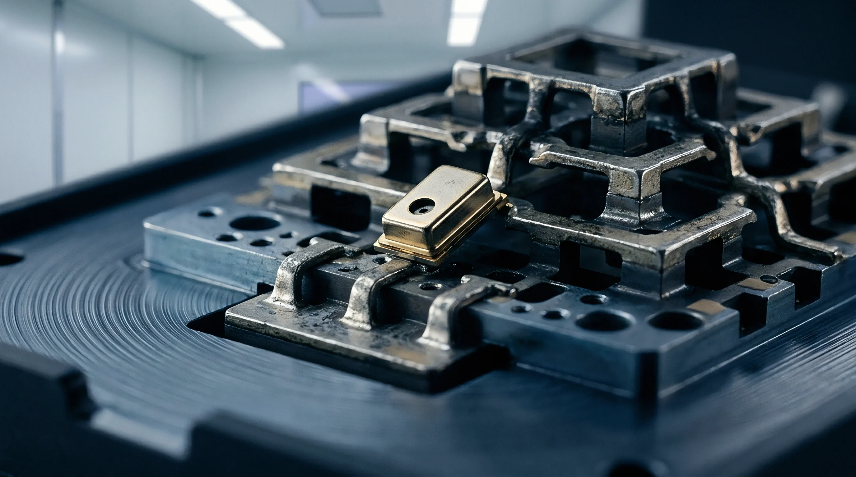
Wireless hardware relies on removable mechanical joints to route RF signals between modules, antennas, and main circuit boards. Spring-loaded pogo pins, U.FL/MHF micro-coaxial connectors, and surface-mount shield cans all require stable mechanical contact to ensure shielding and preserve signal integrity.
A rough ground pad under an RF shield can allows high-frequency electromagnetic field leakage because microscopic gaps between the shield frame and PCB copper act as slot antennas at harmonic frequencies.

Interconnect Architecture in High-Frequency Radios
Board-to-board RF connectors transmit energy through spring contacts pressed against mating pads. High pad roughness breaks the contact area into multiple micro-paths of varying length, and the resulting phase differences introduce sub-nanosecond dispersion and phase jitter in high-speed digital and wideband RF links.
Spring-loaded pins in automated test fixtures or modular radios degrade rapidly when mating against rough PCB pads. Sharp copper asperities act as abrasives, stripping gold plating from the pin tip well before reaching the manufacturer’s rated insertion life.
| Interface Mechanism | Nominal Contact Force (N) | Surface Finish (Ra µm) | Contact Resistance (mΩ) | Return Loss at 5.8 GHz (dB) | PIM Level at 2x20W (dBc) |
|---|---|---|---|---|---|
| Standard Gold Pogo Pin | 0.5 | 0.8 | 45 to 80 | -14 | -95 | Precision Radiated Pogo Pin | 1.5 | 0.2 | 12 to 20 | -24 | -125 | U.FL Receptacle Joint | 2.0 | 0.4 | 15 to 25 | -22 | -118 | SMT Shield Can Frame | 0.1 (per clip) | 1.2 | 110 to 250 | -8 | -75 | Direct Compression Pad | 3.5 | 0.1 | 5 to 10 | -30 | -138 |

Non-Linear Interface Noise and Passive Intermodulation
At high transmit power levels, such as cellular base station feeds or industrial gateway transmitters, rough contact interfaces generate Passive Intermodulation (PIM). This occurs when dense RF current passes through non-linear metal-oxide-metal junctions embedded in rough contact surfaces.
Microscopic oxide films across uncompressed valleys act as non-linear tunnel diodes. When two high-power carriers pass through a rough, oxidized joint, these micro-diodes mix the signals and generate intermodulation products directly within adjacent receiver bands. Third-order products from rough connector joints can raise the receiver noise floor by 20 dB, blinding long-range LoRaWAN or LTE-M receivers.
Per IPC-6012E Class 3 guidelines, surface plating on RF contact lands must maintain a planar profile within 0.15 micrometers to prevent high-frequency intermodulation and localized impedance shifts.
Component vendors frequently attribute high bit error rates to receiver silicon defects when the primary root cause stems from unpolished connector mating surfaces.
- Substrate Profilometry Audit ~ Measure raw PCB contact pad roughness using optical white-light interferometry prior to electroplating deposition.
- Plating Thickness Verification ~ Confirm nickel barrier layer thickness equals a minimum of 3.0 micrometers to prevent copper migration through gold top layers.
- Mechanical Force Alignment ~ Measure static compression force of spring contacts using a calibrated load cell during initial housing assembly.
- RF Impedance Profilometry ~ Run time-domain reflectometry measurements across the mated joint to verify impedance reflections stay within a 50 ohm ± 2 ohm tolerance window.


Plating
Base metals in RF circuit boards and connectors ~ primarily copper and brass ~ oxidize rapidly in air and humidity. Plating with electroplated or immersion metal finishes preserves low contact resistance, but electrodeposited layers mirror the underlying substrate roughness while introducing multi-layer skin depth transitions.
Electroless Nickel Immersion Gold (ENIG) is a common PCB finish, but the underlying nickel layer introduces significant magnetic and resistive losses at radio frequencies.

Metallurgical Stackups and Skin Penetration Layers
With a relative magnetic permeability between 100 and 600, nickel draws RF current directly into its lossy structure. Because nickel’s resistivity is more than four times that of copper, signals traveling through an ENIG-finished rough surface suffer severe attenuation as current passes through the rough nickel barrier to reach the outer gold skin.
Electroless Nickel Electroless Palladium Immersion Gold (ENEPIG) mitigates some of this loss by adding a non-magnetic palladium layer. At millimeter-wave frequencies, direct immersion silver or hard electroplated gold over low-roughness copper eliminates magnetic layers entirely, maximizing energy transfer across contact points.
Gold plating applied over rough nickel substrate fails to reduce RF insertion loss if the RMS roughness exceeds the skin depth of the outer gold layer.

Environmental Corrosion and Contact Degradation over Time
Thin electroplated gold layers contain microscopic pinholes and pores. In humid industrial environments containing sulfur dioxide or chlorine, underlying copper or nickel migrates upward through these pores via galvanic action, forming non-conductive corrosion products across the contact surface.
Surface roughness accelerates pore corrosion by creating stress points during plating where uniform deposition fails. Valleys in rough substrates trap chemical residues, initiating crevice corrosion that degrades contact impedance over months in the field. This degradation can drive contact impedance from tens of milliohms to hundreds of ohms, resulting in complete link failure in low-power wireless modules.
Procurement clauses must specify surface plating parameters, including base copper treatment, nickel barrier thickness, and outer precious metal finish tolerances linked directly to IPC-4552B standards.


Dossier
Maintaining reliable RF contact performance in high-volume module production requires clear drawing callouts, strict material qualifications, and thorough incoming inspection. Specifications relying solely on static DC resistance fail to catch surface roughness defects that degrade high-frequency link margins.
Quality documentation should specify optical surface profilometry alongside traditional mechanical tolerances. Defining maximum peak-to-valley roughness height (Rt) and root-mean-square roughness (Rq) on fabrication drawings prevents board suppliers from using aggressive chemical micro-etching ~ a process often used to improve solder mask adhesion at the expense of RF performance.
Profilometry Enforcement in Volume Hardware Procurement
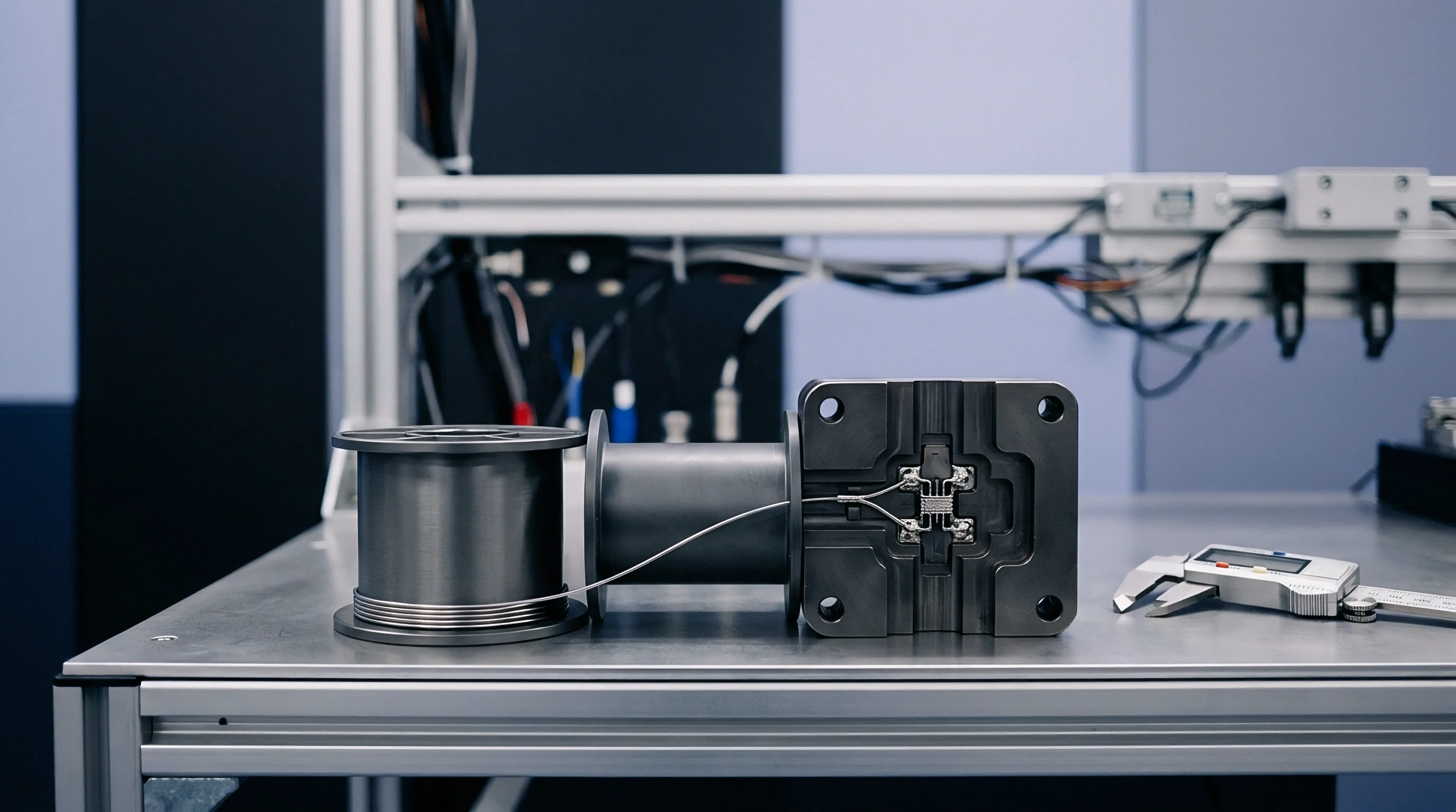
Stylus profilometry drags a physical tip across the surface, but tips with radii above 2 micrometers bridge over narrow valleys, producing artificially optimistic readings. Optical white-light interferometry and confocal laser scanning microscopy offer non-contact 3D mapping capable of resolving sub-nanometer topography across entire RF contact pads.
Incoming inspection procedures should set acceptance thresholds using ISO 25178 surface texture parameters. Tracking Sz (maximum height) and Sa (arithmetic mean height) provides full spatial data, preventing batches with excessive peak heights from reaching the assembly line.
Contact resistance measurements taken under DC conditions fail to indicate RF impedance mismatches caused by microscopic surface topography.
Specification Clauses for High-Frequency Board Layouts
Contracts for radio hardware fabrication should tie board acceptance directly to empirical RF benchmarks. Clear clause definitions are essential to establish liability for yield losses caused by unauthorized substrate or plating process changes.
- Surface Roughness Limits dictate that RF trace contact pads maintain an Rq value below 0.4 micrometers measured per ISO 25178 optical methods.
- Plating Stackup Integrity mandates direct verification of nickel barrier thickness between 3.0 and 6.0 micrometers with zero detectable copper migration pore density.
- Mechanical Retention Tolerance specifies that pogo pin and spring contacts enforce a minimum nominal deflection force of 1.2 Newtons across all operating temperature ranges.
- RF Impedance Verification requires 100 percent coupon testing using Time-Domain Reflectometry to confirm contact reflection coefficients stay below -20 dB up to target operating frequencies.
Will future millimeter-wave modular hardware designs transition entirely away from mechanical spring joints toward direct fused metallic interconnections to bypass physical surface roughness limits entirely?