Thermal Compensation Mechanics in Real Time Clock Oscillators
Integrated real-time clock thermal compensation uses digital capacitor arrays to counter parabolic quartz drift, keeping sleep clock drift below 2 ppm.

Physics
Standard 32.768 kHz tuning fork quartz crystals drift in frequency as temperature shifts, primarily because mechanical deformation alters their resonance. Their X-cut geometry prioritizes small size and minimal power draw over thermal stability, causing resonant frequency to follow a quadratic parabola centered on a turnover temperature. Frequency deviation in parts per million is modeled by:
f_error = -B (T – T_0)^2
The parabolic temperature coefficient B typically falls between 0.034 and 0.040 parts per million per degree Celsius squared. Turnover temperature T_0 is set by the physical cut angle, nominally centered at 25 degrees Celsius within a tolerance of plus or minus 5 degrees Celsius.
Operating outside room temperature pulls the resonant frequency downward whether the crystal heats up or cools off. At minus forty degrees Celsius ~ a sixty-five degree offset from turnover ~ the parabolic equation yields a frequency drift of -147.875 parts per million, causing an uncompensated real-time clock to lose 12.77 seconds per day. At plus eighty-five degrees Celsius, the parabolic curve causes the exact same drop.
The table below outlines how uncompensated parabolic quartz drift scales across common operating temperatures when B equals 0.035 parts per million per degree Celsius squared.
| Temperature (Degrees Celsius) | Delta T from Turnover (Degrees Celsius) | Calculated Frequency Drift (ppm) | Daily Time Accumulation Error (Seconds) |
|---|---|---|---|
| -40 | 65 | -147.88 | -12.78 |
| -20 | 45 | -70.88 | -6.12 |
| 0 | 25 | -21.88 | -1.89 |
| 25 | 0 | 0.00 | 0.00 |
| 50 | 25 | -21.88 | -1.89 |
| 70 | 45 | -70.88 | -6.12 |
| 85 | 65 | -147.88 | -12.78 |
Other material factors degrade frequency stability alongside parabolic drift. Physical aging alters the baseline turnover frequency over time as mechanical stresses relax and trace contaminants outgas inside the metal package. Aging shifts frequency by plus or minus 3 parts per million in the first year, slowing to roughly 1 part per million per year after that.
Physical shock introduces microscopic lattice strain that permanently alters crystal stiffness, while drive levels over 1 microwatt trigger drive-level dependency, shifting the turnover temperature and degrading overtone suppression.
Whether stress relaxation in crystal mounting adhesives over a ten-year operating lifespan permanently shifts the turnover temperature beyond what digital compensation can correct remains a subject of ongoing discussion.


Layout
Integrated real-time clock ICs replace discrete quartz circuits with active thermal compensation on the same die. These temperature-compensated oscillators counteract parabolic drift either by adjusting the load capacitance seen by the quartz resonator or by altering internal clock division ratios. Because elevated ambient temperatures degrade output stability, the compensation circuit relies on an accurate temperature sensor placed close to the quartz blank.
Switched Capacitor Tuning Networks
Analog compensation pulls the crystal frequency upward by trimming load capacitance C_L. Modern architectures integrate binary-weighted switched capacitor arrays directly on the silicon die. A high-resolution bandgap sensor measures die temperature and feeds digitized readings to a compensation engine, which calculates or looks up the needed offset and toggles solid-state switches in the array.
Lowering total load capacitance increases oscillation frequency to offset parabolic drop, while internalizing the array eliminates external stray capacitance.
A switched capacitor array pulling an integrated 32.768 kHz crystal holds frequency error within 2 ppm across industrial temperature limits from minus forty to plus eighty-five degrees Celsius.
Digital Pulse Trimming Mechanics
Digital frequency trimming leaves the quartz crystal running at its uncompensated resonant frequency and corrects timekeeping by dropping or inserting clock pulses at the primary counter. A programmable fractional divider suppresses a set number of 32.768 kHz cycles over a sixty-second window. While this avoids altering oscillator load impedance ~ preserving low power startup behavior ~ pulse suppression introduces sub-second clock phase jitter equal to one full cycle period of 30.5 microseconds, making raw digital trimming unsuitable for radio baseband timing.
| Architecture Type | Active Sensing Current | Compensation Step Size | Phase Jitter Impact | PCB Trace Sensitivity |
|---|---|---|---|---|
| Switched Capacitor Array | 450 nA to 850 nA | 0.1 ppm to 0.5 ppm | Zero phase discontinuity | Low when integrated in module |
| Digital Pulse Suppression | 200 nA to 400 nA | 0.12 ppm to 1.0 ppm | 30.5 microsecond clock jitter | High on external crystal traces |
| Varactor Analog Tuning | 1.2 uA to 3.0 uA | Continuous analog step | Low phase noise penalty | Moderate trace sensitivity |
Integrated real-time clock modules enclose the compensation engine, temperature sensor, switched capacitor array, and quartz crystal inside a single hermetic ceramic package. This integration avoids the trace parasitic uncertainties that complicate discrete board layouts.
- Integrated Load Capacitance eliminates external tuning capacitors by placing die-level capacitor banks directly across crystal terminals, saving board space and minimizing parasitic loading.
- On-Chip Bandgap Sensing positions the temperature sensing diode within hundreds of micrometers of the crystal mounting pad to reduce thermal response lag.
- Register-Driven Pulse Trimming uses factory-calibrated polynomial constants stored in non-volatile memory to compute real-time switch settings for the capacitor matrix.
Packaging the crystal directly with the compensation network allows manufacturers to match capacitor banks to the specific blank during assembly, eliminating board-level parasitic mismatch.

Budgets
Sleep energy accounting in battery-powered wireless nodes depends heavily on clock current during extended idle states. Uncompensated 32.768 kHz crystal drivers draw 40 to 100 nanoamperes of continuous bias current. Temperature-compensated modules draw higher baseline current because of periodic sensor readouts and calculation logic, but uncompensated sleep clock drift forces receiver listening windows to widen significantly.
Energy Costs of Autonomous Polling
Integrated thermal compensation engines run on fixed polling schedules. Each conversion cycle powers up the bandgap sensor, runs an analog-to-digital conversion, computes polynomial corrections, and updates the switched capacitor array. These measurement bursts draw 20 to 50 microamperes for 2 to 10 milliseconds.
Lengthening the polling interval lowers average current draw, but leaves the system more vulnerable to rapid thermal transients.
Consider the trade-offs for an industrial tracking node powered by a 2.2 Ampere-hour primary lithium thionyl chloride battery with a ten-year target service life and a sleep current budget of 2.5 microamperes. An uncompensated real-time clock draws just 50 nanoamperes continuously. However, across an outdoor temperature range of minus thirty degrees Celsius to plus sixty degrees Celsius, drift reaches 120 parts per million.
When the endpoint wakes for a scheduled down-link window, the receiver must open early to cover that cumulative drift.
Over a 60-second sleep interval, 120 parts per million drift produces a timing uncertainty of plus or minus 7.2 milliseconds, forcing the receiver to stay active for 14.4 milliseconds to catch transmissions reliably. Drawing 15 milliamperes in active receive mode, that extra 14.4 milliseconds every 60 seconds adds an average current penalty of 3.6 microamperes. Total timing consumption reaches 3.65 microamperes, overshooting the sleep current budget by 46 percent.
Compliance with European telecommunications standardization requirements for short range devices limits duty cycle allocations, forcing receivers that miss timing windows into prolonged channel listening states that drain battery reserves.
Replacing the uncompensated oscillator with an integrated temperature-compensated RTC module changes the energy calculation. The compensated module draws 650 nanoamperes continuously while polling temperature every 16 seconds, holding frequency drift within 2 parts per million across the full temperature range. Timing uncertainty over a 60-second sleep interval drops to 0.12 milliseconds, shrinking the required receive window to 0.24 milliseconds.
The receiver wake penalty falls to 0.06 microamperes, bringing total timing current to 0.71 microamperes ~ well below the 2.5-microampere threshold.
Using an uncompensated clock in primary-lithium endpoints with low active duty cycles drains batteries prematurely, leading to unexpected connection drops and shortened device lifespans in outdoor deployments.

Protocols
Baseband timing precision determines how long a receiver search window must remain open for radio synchronization. Lower clock accuracy forces wireless modems to wake earlier and remain active longer to ensure preamble capture, making real-time clock performance a direct driver of RF energy consumption during sleep intervals in standards like Bluetooth Low Energy, LoRaWAN, LTE-M, and NB-IoT.
How Does Clock Drift Inflate Protocol Listen Windows?
Wireless protocol standards define receive window widening based on sleep clock accuracy specifications. The window length follows the relation:
T_window = 2 (Drift_local + Drift_remote) T_sleep + T_preamble_margin
Here Drift_local represents receiver clock uncertainty in parts per million, and Drift_remote represents base station clock uncertainty. As drift rises, T_window expands linearly, increasing RF front-end energy consumption during every sleep-wake cycle.
| Wireless Standard | Nominal Sleep Interval | Uncompensated Clock Drift Window | TCXO Clock Drift Window | Receiver Energy Penalty |
|---|---|---|---|---|
| LoRaWAN Class A (SF12) | 128 Seconds | 38.40 Milliseconds | 0.51 Milliseconds | +75 Millijoules per RX slot |
| Bluetooth Low Energy | 4.0 Seconds | 4.00 Milliseconds | 0.016 Milliseconds | +0.06 Millijoules per event |
| LTE-M eDRX Mode | 40.96 Seconds | 12.28 Milliseconds | 0.16 Milliseconds | +0.25 Millijoules per paging cycle |
| NB-IoT PSM Mode | 24 Hours | 25.55 Seconds | 0.35 Seconds | +3.8 Joules per re-attach scan |

Sub-Gigahertz Duty Cycles and Preamble Alignment
LoRaWAN Class A endpoints sleep between uplink transmissions and open two receive windows, RX1 and RX2, at fixed offsets afterward. At Spreading Factor 12, symbol duration is 32.77 milliseconds, and preamble detection requires tight symbol boundary alignment. Cumulative timing error exceeding half a symbol duration results in preamble loss and dropped downlink frames.
An uncompensated crystal drifting by 150 ppm over a long sleep window misses the downlink frame completely unless the receiver extends listening across multiple symbol periods.
Tighter real-time clock accuracy shrinks receiver wakeup margins, directly converting timing precision into RF energy savings.
Cellular Power Saving Modes and Extended Discontinuous Reception
Cellular IoT devices running on LTE-M or NB-IoT networks rely on Power Saving Mode and extended Discontinuous Reception (eDRX) to meet multi-year battery targets. In eDRX mode, devices sleep for up to 40.96 seconds while maintaining network registration. If clock drift pushes timing past the paging window threshold, the endpoint misses the network page.
Missing a page triggers a full cell search, driving the RF power amplifier up to plus 23 dBm to re-acquire synchronization ~ a process that draws 100 to 250 milliamperes over several seconds and decimates battery budgets.
Software timing resynchronization can compensate for oscillator instability, though extra preamble transmissions carry substantial energy overhead.

Bench
Verifying thermal compensation accuracy requires testing physical clock hardware under controlled environmental ramps in precise temperature chambers. Room-temperature bench tests fail to capture response lag between on-chip sensors and encapsulated quartz blanks, where dynamic thermal changes introduce tracking error and localized gradients offset sensor readings.
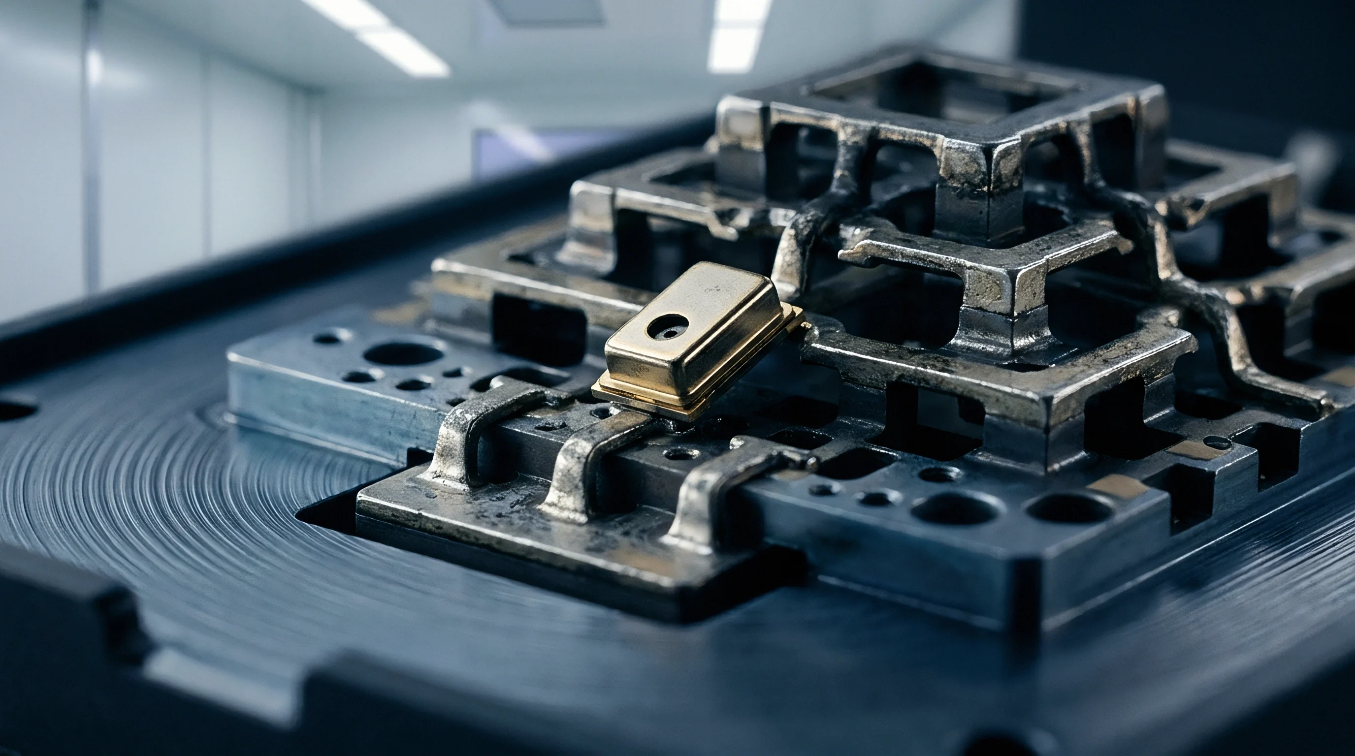
Chamber Sweeps and Dynamic Hysteresis Characterization
Static equilibrium tests evaluate clock accuracy only after temperatures settle, missing hysteresis caused by differential expansion stress in the ceramic package and internal thermal gradient lags. Qualification testing requires continuous temperature sweeps to reveal true dynamic performance.
- Place the device under test in a programmable thermal chamber connected to an external high-stability frequency counter referenced to a rubidium timebase.
- Set the chamber to ambient room temperature and record baseline output frequency across a thirty-minute thermal soak.
- Ramp chamber temperature down to minus forty degrees Celsius at a maximum rate of one degree per minute while taking continuous frequency measurements.
- Hold at minus forty degrees Celsius for one hour to establish full thermal equilibrium across the packaging.
- Ramp temperature up to plus eighty-five degrees Celsius at the same sweep rate while logging the hysteresis curve.
- Calculate thermal gradient error by comparing frequency shifts during continuous ramps against static equilibrium hold points.
Thermal gradients across printed circuit boards offset integrated temperature sensors from the quartz blank, creating temporary frequency errors during rapid ambient temperature shifts.
Thermal gradient mapping requires placing thermal sensors directly on the real-time clock package while monitoring power dissipation in neighboring components. High-power microcontrollers, charger ICs, and RF power amplifiers produce rapid local heating. If a power amplifier generates a 10 degrees Celsius jump within two seconds, heat flows through the ground plane into the clock package.
The ceramic enclosure transfers heat to the silicon temperature sensor faster than it reaches the encapsulated quartz blank. Reading an elevated die temperature, the compensation engine applies correction capacitors prematurely, creating transient frequency errors up to 10 parts per million until internal equilibrium normalizes.
Including mandatory thermal hysteresis sweep requirements in component qualification specifications ensures module suppliers warrant drift limits across dynamic temperature transitions rather than static equilibrium points alone.

Sourcing
Selecting low-power timing components requires balancing initial bill-of-materials cost against operational reliability in the field. Discrete 32.768 kHz crystals paired with microcontroller internal RTCs offer a lower upfront component price, while integrated RTC modules cost more initially but eliminate hidden firmware overhead and reduce board-level scrap.
Discrete Quartz Crystal Selection versus Integrated Modules
Discrete crystals cost between 0.05 and 0.15 USD in high volume. However, using a discrete crystal requires adding external load capacitors, routing sensitive high-impedance traces, and spending software engineering time on firmware compensation. Microcontroller RTCs lack factory-calibrated load banks, forcing firmware to read external thermistors, calculate parabolic equations, and write adjustments to trim registers.
This software approach cannot compensate for board parasitic shifts, component lot variations, or steep thermal gradients across the assembly.
Integrated temperature-compensated RTC modules cost between 0.80 and 2.20 USD in volume. During assembly, module manufacturers perform single- or multi-point thermal calibration across the industrial temperature range and burn correction constants into non-volatile memory. Hermetic ceramic packaging isolates the resonator from environmental influences.
These modules guarantee drift bounds within 2 to 5 parts per million out of the box, shifting timing accuracy liability from the device integrator to the component vendor.
Component Yield and Production Line Qualification
Sourcing teams evaluating timing options assess supplier quality using specific manufacturing metrics:
- Frequency Tolerance Binning screens raw blanks at 25 degrees Celsius, rejecting crystals with turnover frequency offsets over plus or minus 10 parts per million before packaging.
- Stray Capacitance Allocation restricts internal routing parasitic variation to under 0.2 picofarads across assembly lots.
- Reflow Thermal Profile Survival sets maximum frequency shift limits under standard lead-free reflow, requiring post-reflow stability within plus or minus 1 part per million.
- Hermetic Package Leak Rates verifies fine-leak helium mass spectrometry down to 10^-8 cubic centimeters per second to prevent internal oxidation over a ten-year lifespan.
Clock selection ultimately defines the system power budget. Using integrated temperature-compensated RTCs converts timing accuracy from a variable driven by thermal environment into a fixed design constraint. Narrower receiver search windows lower field failure rates, protect protocol timing margins, and make product costs more predictable across high-volume production runs.