Basic Modular Regulatory Compliance for Scale Hardware Manufacturing
Modular regulatory compliance reduces host re-testing by transferring radio approvals, but demands strict adherence to reference trace geometry and power decoupling.


Shield
Designing radio frequency equipment relies on physical isolation to keep electromagnetic interference within predictable limits. When integrating pre-approved radio subassemblies into host hardware, physical shielding serves as the primary barrier between certified transmitter circuits and surrounding host electronics. Under Title 47 Part 15.212, Federal Communications Commission rules require a modular transmitter to carry its own RF shielding directly over its emitting circuitry.
This cover prevents parasitic coupling between host power rails, processor clocks, and the module’s internal local oscillator. Without it, emissions from host components mix into the radio circuitry, generating uncertified spurious outputs that invalidate the module’s baseline pre-certification.
High-volume manufacturing lines rely on surface-mount radio modules built with nickel-silver or tin-plated steel shield cans soldered directly to the module ground plane. These cans prevent external electrostatic fields from modulating sensitive phase-locked loops in the RF transceiver, while decoupling capacitors sink high-frequency noise. If a module vendor omits this metal cover to trim unit costs, the subassembly forfeits full modular approval and falls back to limited modular status, shifting the burden of compliance testing onto the host hardware program.

Physical Enclosure Mechanics and Field Isolation
Enclosing transmitter circuits in solid metal barriers prevents radiated leakage across host circuit boards. These covers require continuous solder contact around their perimeter to seal the ground seam against microwave energy leakage. Any gap larger than one-twentieth of the operating wavelength acts as a slot antenna, letting internal harmonics escape into host enclosure cavities while unshielded inductors radiate magnetic energy into nearby traces.
When host ground planes fail to absorb return currents ~ such as when noisy switching converters sit directly beneath an unshielded module area ~ voltage ripple couples into the power amplifier, causing sideband spur failures during radiated emissions scans.

Power Supply Decoupling and Buffered Interfaces
Transmitter stability depends on clean voltage rails entering the radio module subsystem. Title 47 Part 15.212 mandates on-module power supply regulation so host voltage fluctuations cannot shift transmitter frequency or output power. If host supply lines carry ripple exceeding 50 millivolts peak-to-peak, internal regulators struggle to maintain carrier frequency stability.
On digital control lines, buffered inputs stop host microcontrollers from driving signals past rated logic levels, preventing long PCB traces from acting as parasitic antennas before ferrite beads can suppress high-frequency noise. Direct access to unbuffered synthesizer tuning lines leaves the carrier vulnerable to host crosstalk, which can spoil carrier purity and force regulatory re-qualification.
On-module metallic covers do not eliminate the need for host-level emissions testing, as unshielded board features can still trigger failures during accredited laboratory scans.


Grant
The choice of regulatory authorization path dictates how compliance responsibilities are divided between the module vendor and the host manufacturer. Full modular approval allows a radio subassembly to be integrated into diverse host enclosures without re-running intentional radiator certification tests. Limited modular approvals apply whenever a module lacks internal power regulation, metal shielding, or a fixed antenna structure.
Under a limited grant, the vendor’s authorization is conditional, forcing host hardware teams to execute Class II Permissive Changes or apply for new equipment authorizations for each distinct host enclosure layout.
When impedance shifts distort transmission lines and generate spurious harmonics, host manufacturers using limited modular units bear full testing liability across every product variant. The table below outlines operational parameters, lab testing requirements, and document ownership structures for the main wireless modular authorization paths.
| Scope Parameter | Full Modular Approval | Limited Modular Approval | Discrete Transceiver Circuit |
|---|---|---|---|
| Module Metal Shielding | Mandatory full perimeter shield can | Optional or partial enclosure shield | None; host board provides shielding |
| On-Module Power Regulation | Mandatory dedicated low-dropout regulator | Host board supplies regulated rail | Host board supplies regulated rail |
| Antenna Connection Format | Unique connector or printed trace | Host-routed microstrip line | Host-routed microstrip line |
| Initial Non-Recurring Lab Expense | Covered by module supplier | Shared between vendor and host maker | 100 percent funded by host maker |
| Host Radiated Emissions Testing | Unintentional radiator verification only | Full intentional radiator testing | Full intentional radiator certification |
| Regulatory Grant Ownership | Module vendor holds FCC ID / CE TCF | Module vendor holds conditional ID | Host manufacturer holds FCC ID / TCF |

Regulatory Authorization Boundaries across Regional Jurisdictions
Wireless device approvals operate under distinct legal frameworks across North America, Europe, and Asia-Pacific. In the United States and Canada, the Federal Communications Commission and Innovation, Science and Economic Development Canada issue discrete Grant certificates linked to specific equipment IDs. In contrast, radio equipment brought to market in Europe under the Radio Equipment Directive 2014/53/EU does not receive a central government grant; compliance relies on a manufacturer Declaration of Conformity backed by a Technical Construction File.
Installing a CE-marked module inside a host enclosure requires the host manufacturer to assess the combined product against relevant harmonized standards, such as ETSI EN 300 328 for 2.4 GHz wideband data systems and ETSI EN 301 489 for electromagnetic compatibility.

Amortization Dynamics of Modular Hardware Certification
Selecting pre-certified wireless modules trades higher bill-of-materials costs for lower non-recurring engineering expenses. Designing a discrete radio onto a host motherboard typically demands $35,000 to $60,000 in lab fees and three months of schedule risk to complete FCC Part 15 Subpart C certification and European Notified Body review. Pre-certified modules reduce host testing to unintentional radiator verification under FCC Part 15 Subpart B, which runs between $4,500 and $8,000.
Production volumes over 100,000 units annually often justify discrete designs to eliminate vendor markups, whereas runs under 30,000 units usually achieve lower total landed costs by paying the module premium to bypass upfront lab risk.
ETSI EN 301 489-17 requires host systems incorporating wireless modules to undergo combined radiated immunity evaluation under maximum RF throughput conditions.
Section 15.212(a)(1)(vi) of Title 47 in the Code of Federal Regulations requires modular transmitters to display their own FCC ID, placing explicit end-product labeling responsibilities on the host manufacturer’s compliance documentation.

Trace
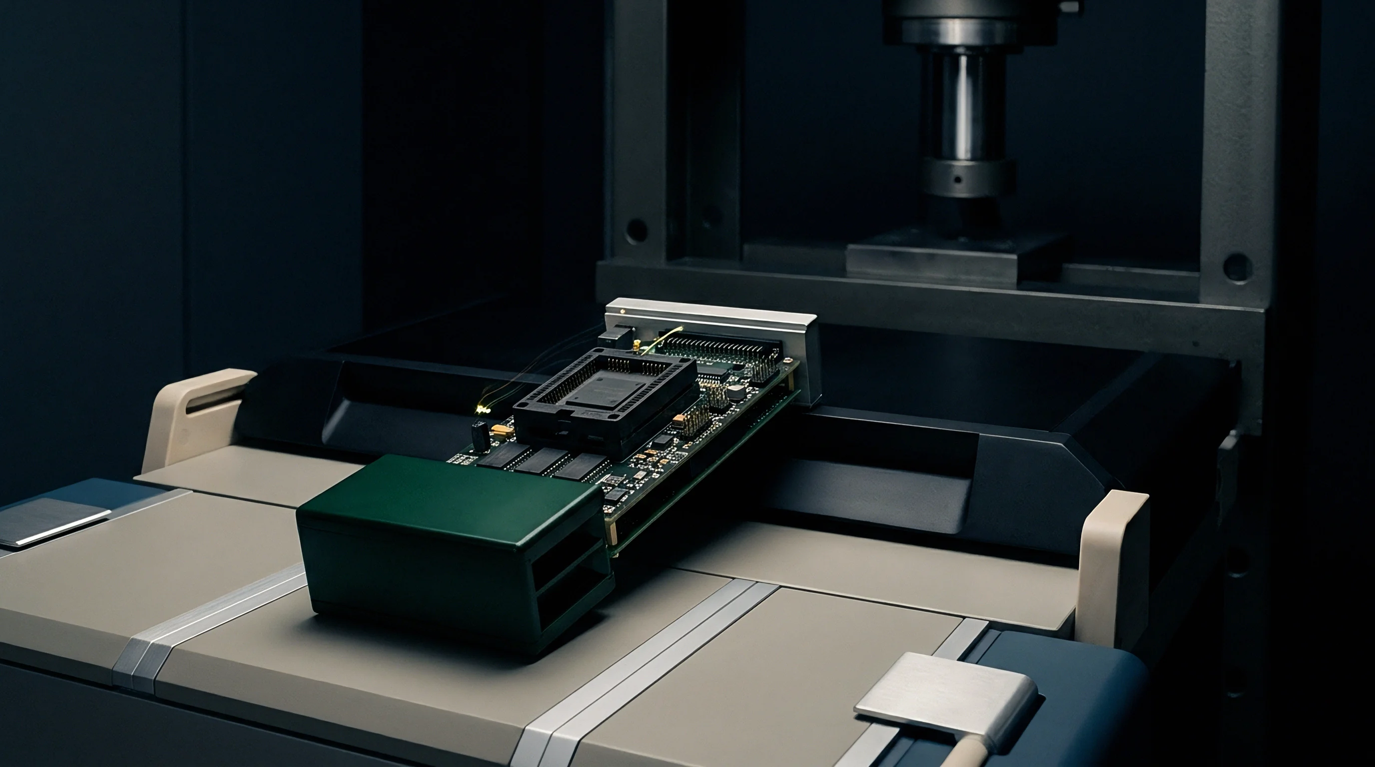
High-frequency signal paths between transceiver ICs and antenna launch structures require strict manufacturing tolerances. When a radio module uses an external antenna pin instead of an onboard ceramic chip antenna, the PCB trace connecting that pin to the host antenna connector becomes an integral part of the certified antenna system. Module vendors specify exact layout geometry in their grant filings, including Gerber files, substrate dielectric constants, copper weight, and coplanar microstrip dimensions.
Any departure from these published reference specs invalidates the module’s pre-certification, treating the assembly as an uncertified radio circuit on the host board.
Because impedance mismatches cause RF power loss and improper grounding distorts antenna radiation patterns, board fabrication shops must hold dielectric thickness within ±5 percent across production lots. The list below details key layout parameters hardware engineers must maintain to preserve valid modular transmitter grants.
- Controlled Impedance Microstrip Geometry Maintaining a precise 50-ohm characteristic impedance prevents signal reflection back into the power amplifier stage.
- Keep-Out Layer Cleanliness Keeping ground plane voids clear underneath antenna structures preserves the intended radiation pattern without capacitive loading.
- Ground Via Perimeter Density Placing ground vias closer together than one-tenth of the operating wavelength keeps high-frequency currents contained along the RF trace.
- Transmission Line Routing Radius Using smooth curved trace bends avoids sharp impedance discontinuities that radiate harmonic energy inside the host.

Coplanar Waveguide Layout Geometry and Impedance Matching
Designing consistent transmission lines requires careful balancing of conductor width and ground clearance. Ground-backed coplanar waveguides deliver high signal isolation on multi-layer FR-4 boards. For instance, a standard 4-layer stack-up with a 0.2 mm outer dielectric requires a 0.32 mm trace width separated by a 0.2 mm gap from adjacent copper to hit 50-ohm characteristic impedance at 2.4 GHz.
Cutting thermal relief slots into the underlying RF ground plane disrupts return current paths and shifts impedance, spiking unwanted harmonic emissions during transmit bursts and altering near-field coupling once installed in host enclosures.

Is Host Re-Testing Mandatory after Antenna Trace Modifications?
Modifying RF conductor routing on host PCBs invalidates the vendor’s original test filings. If a design team repositions an RF connector or switches substrate materials from FR-4 to high-frequency Rogers laminates, the host manufacturer must submit a Class II Permissive Change. This process requires updated Gerber files and test data from an accredited lab showing that spurious emissions and band-edge performance still meet statutory limits under the new trace layout.
Should the modified trace produce higher peak gain or worse spurious emissions than the original reference layout, regulators will reject the permissive change, requiring a full equipment authorization under a new Grantee code.
Matching host PCB dielectric properties to the vendor reference specification keeps RF trace emissions within certified limits.


Chamber
Calibrated test environments provide the baseline needed to measure unwanted radio frequency radiation accurately. Semi-anechoic chambers lined with ferrite tiles and RF absorbers shield the hardware under test from external interference such as cellular signals and broadcast stations. Compliance testing for host assemblies containing modular radios focuses on measuring radiated spurious emissions up to the tenth harmonic of the highest internal clock frequency.
For North America, ANSI C63.4 specifies these measurement procedures, mandating antenna distances of 3 meters or 10 meters within calibrated facilities.
When ground connections weaken, high-speed digital traces near enclosure seams readily act as unintended radiators. The table below outlines standard regulatory test parameters and pass/fail thresholds enforced during host-level compliance scans for both intentional and unintentional radiators.
| Test Parameter | FCC Part 15 Subpart B (Class B) | ETSI EN 300 328 (RED) | Host Impact Strategy |
|---|---|---|---|
| 30 MHz to 88 MHz Limit | 40.0 dBuV/m quasi-peak at 3m | -36 dBm ERP (100 kHz BW) | Filter high-current DC-DC converter inputs |
| 88 MHz to 216 MHz Limit | 43.5 dBuV/m quasi-peak at 3m | -36 dBm ERP (100 kHz BW) | Damp high-speed memory clock harmonics |
| 216 MHz to 960 MHz Limit | 46.0 dBuV/m quasi-peak at 3m | -36 dBm ERP (100 kHz BW) | Add grounding fingers to metal enclosure joints |
| 1 GHz to 40th Harmonic | 54.0 dBuV/m average at 3m | -30 dBm ERP (1 MHz BW above 1GHz) | Shield high-frequency trace launch paths |
| Conducted Line Emissions | 46 to 56 dBuV quasi-peak (150kHz-5MHz) | Not directly applicable to DC subassemblies | Place common-mode chokes on power inlets |
Radiated Spurious Emission Diagnostics and Harmonic Spikes
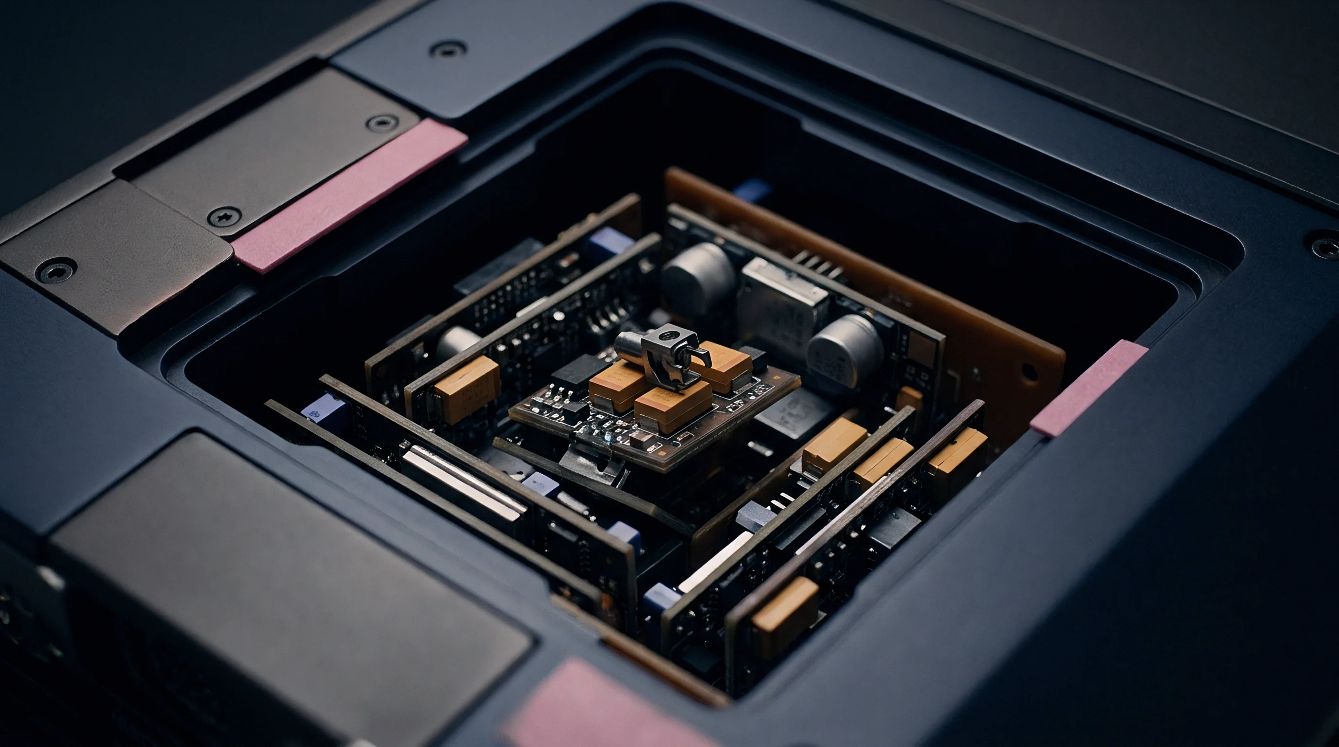
Unintended radio emissions tend to peak at harmonic multiples of the fundamental frequency during high-power transmission. When a host system pairs a 2.4 GHz Wi-Fi module with a high-speed ARM application processor, 400 MHz clock signals can mix with the RF carrier to generate intermodulation products. Pinpointing these noise sources usually requires near-field magnetic probe scans before committing to full chamber sweeps.
Adding ferrite beads to flex cables suppresses common-mode noise moving from the motherboard to displays or battery wiring, keeping internal cabling from acting as dipole antennas inside the chamber.

Worked Chamber Test Budget for Multi-Radio System Verification
Deploying dual wireless links introduces specific time and test costs during host compliance validation. Take, for example, an industrial gateway board carrying a pre-certified LTE Category-M cellular module alongside a 2.4 GHz Bluetooth Low Energy module. Verifying host-level compliance while preserving the existing modular grants requires chamber testing at an accredited 3-meter facility charging $350 per hour.
The test plan covers three operational modes: dual active transmission, single transmission, and receiver standby. Sweeping radiated emissions from 30 MHz to 26.5 GHz takes 8 hours per mode across four board orientations (0, 90, 180, and 270 degrees). These combined scans require 24 total chamber hours, racking up $8,400 in direct lab fees.
Engineering evaluation and test setup add another $2,000. If the board fails Class B limits by 2.4 dB at 800 MHz because of ungrounded heat sink resonances, engineers might spend 4 hours troubleshooting with ferrite clips, adding $1,400. That brings total chamber costs to $11,800 before compiling the Technical Construction File.
Radiated emissions exceeding Class B limits by 3 dB at harmonic peaks frequently trace back to ungrounded heat sinks or noisy switching regulators rather than module transmitter failure.
Failing radiated emissions scans during final integration forces board spins, delays volume shipments, and incurs repeat lab fees.


Filing
Submitting official documentation to spectrum regulators provides the legal authorization needed to sell wireless hardware. Importers and manufacturers file certification packages with Telecommunication Certification Bodies in the United States or assemble Technical Construction Files within the European Economic Area. Under modular grants, host manufacturers must retain test reports proving the host enclosure has not altered certified radio parameters.
These filings legally commit the vendor to maintain identical physical build standards across every production unit.
The procedure below details the administrative steps needed to compile regulatory compliance records for commercial hardware distribution.
- Audit supplier radio test reports against host operating frequency bands and internal thermal limits.
- Confirm that host antenna peak gain does not exceed parameters authorized in the transmitter grant.
- Execute spot-check radiated spurious emissions testing inside an accredited anechoic environment prior to mass assembly.
- Compile technical construction dossiers containing schematics, layout Gerber files, and signed declarations of conformity.
- Archive regulatory approval documentation for ten years post-production across all target commercial markets.

Technical Construction File Management under European Standards
Companies selling wireless hardware in European markets must retain full engineering records for regulatory inspection. Under the Radio Equipment Directive, a Technical Construction File includes host PCB schematics, bills of materials, risk assessments, user manuals, and test data covering both the radio module and host unintentional emissions. This dossier must stay available to enforcement authorities for ten years after the final unit leaves the factory.
If a supplier swaps passive components on the radio module without formal notice, the file loses legal standing, exposing the importer to product recall actions.

Permissive Change Classifications for Equipment Modification
Changes to certified radio circuitry mandate specific filing pathways depending on how significantly the hardware is altered. Under 47 CFR 2.1043, the Federal Communications Commission defines Class I and Class II Permissive Changes. Class I covers minor circuit tweaks that do not increase radiated emissions or alter thermal behavior, requiring no formal filing with a Telecommunication Certification Body.
Class II applies when modifications slightly increase radiated emissions while staying within legal limits, or when co-locating multiple transmitters within 20 centimeters of one another. Class II changes require submitting updated documentation and accredited lab test data prior to shipping modified hardware.
Integrating an approved transmitter into a host enclosure under 20 cm user separation distance shifts device classification from mobile to portable, forcing SAR evaluation regardless of prior modular approvals.
Whether regional spectrum regulators will standardize radio software authorization across international markets remains an open question for cross-border hardware programs.


Duty
Legal responsibility for compliance rests entirely with the company distributing the finished product. Customs agencies and spectrum regulators hold the Importer of Record or brand owner liable for non-compliant RF emissions, regardless of any guarantees given by a module supplier. Hardware brands sourcing white-label subassemblies or turnkey hardware from contract manufacturers must independently verify that supplier grants remain active and match the exact silicon revisions used on production lines.
Because subcontracting manufacturing does not shift legal liability, contracts must clearly define how technical responsibilities are divided if compliance issues arise in commercial channels. The list below outlines key vetting criteria brand owners should enforce before selecting modular radio suppliers.
- Grantee Code Transparency Verification of the vendor equipment authorization identity on official regulatory databases confirms active grant status.
- Antenna Reference Gerber Availability Complete CAD files and stack-up specifications allow exact reproduction of the test trace geometry on host boards.
- Firmware Lock Architecture Regulatory parameters embedded in locked memory prevent host software from driving transmission past approved output limits.
- Component Change Notification Terms Contractual guarantees of ninety days advance notice for passive component substitutions protect filing validity.

Contractual Allocation of Compliance Liabilities
Supply agreements distribute financial risk when finished hardware fails post-assembly audits. Procurement contracts should require module vendors to indemnify brand owners against recalls triggered by unannounced subassembly component changes. If a vendor swaps out an RF filter to cut costs and shifts out-of-band harmonics as a result, host systems using that module risk market bans.
Contracts must make suppliers responsible for re-testing fees, scrapped inventory, and customs holding costs linked to invalid certification filings.

Bill of Materials Freeze and Change Notification Control
Freezing the bill of materials ensures radio performance remains consistent across high-volume production runs. Contract manufacturers often look for cheaper equivalents for passive capacitors, inductors, and crystal oscillators. But in high-frequency RF designs, substituting even a ceramic capacitor with one having higher equivalent series resistance can shift tuning resonances and increase spurious emissions.
Strict Engineering Change Order policies prevent factory purchasing teams from altering component specifications without written approval from the brand owner’s engineering team.
Contract manufacturing agreements that explicitly assign component notification obligations to the assembly plant prevent unannounced passive substitutions from invalidating filed transmitter test reports.