De Embedding System Scatter Parameters across Contract Manufacturing Production Lines
De-embedding high-frequency S-parameters on production lines requires IEEE 370 2x-thru calibration, automated fixture removal, and continuous contact wear tracking.


Fixture
At frequencies beyond 10 GHz, evaluating printed circuit assemblies requires direct vector network analysis at the component contact pads. While standard co-axial cables from a Vector Network Analyzer (VNA) terminate at panel connectors, the Device Under Test (DUT) interfaces through microstrip traces, coplanar waveguides, spring probes, or ball grid array landing pads. These physical transitions introduce parasitic inductance, shunt capacitance, insertion loss, and phase delays that corrupt raw scatter parameter (S-parameter) measurements.
Until these channel artifacts are stripped away, production line tests measure the test interface rather than the component itself.
RF energy reflects wherever impedance changes, while electrical lengths inside test channels shift phase angle readings. On high-volume production lines, physical test interfaces degrade over thousands of insertion cycles. Isolating and removing these measurement errors depends on mathematical de-embedding ~ a process that extracts the two-port or multi-port scatter matrix of the device from the surrounding fixture environment.
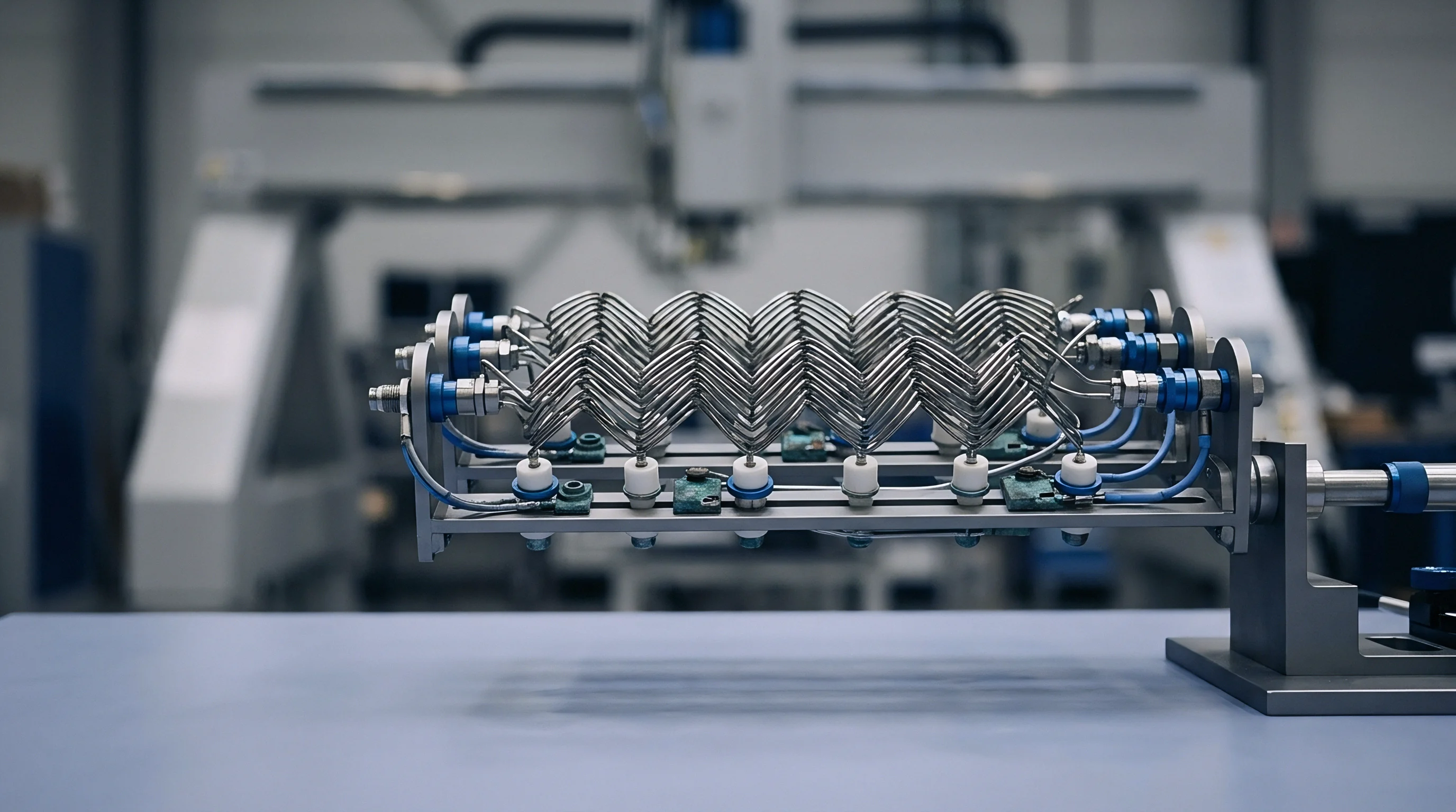
Launch Design and Microstrip Discontinuities
Transitioning from co-axial to planar structures alters wave propagation modes from transverse electromagnetic to microstrip or conductor-backed coplanar modes. Discontinuities at SMA, 2.92 mm, or 1.85 mm connector launches distort local electric and magnetic fields. Near the launch pin, higher-order modes excite reactive parasitic components that show up as sharp return loss spikes on raw S11 sweeps ~ an effect further complicated by PCB substrate tolerances across manufacturing lots.
Dielectric constant variation shifts transmission line impedance. A target 50-ohm microstrip trace varies between 46 ohms and 54 ohms when glass weave density fluctuates or resin content shifts during lamination. Test fixtures built on low-cost FR-4 laminates exhibit high dissipation factors, attenuating high-frequency S21 transmission signals by several decibels per inch at millimeter-wave bands.
High-frequency contract manufacturing lines instead use hydrocarbon ceramic or polytetrafluoroethylene laminates for test interface boards, maintaining controlled dielectric properties up to 40 GHz.
Physical measurement reference planes shift faster than Vector Network Analyzer calibration schedules when test sockets undergo mechanical compression cycles.
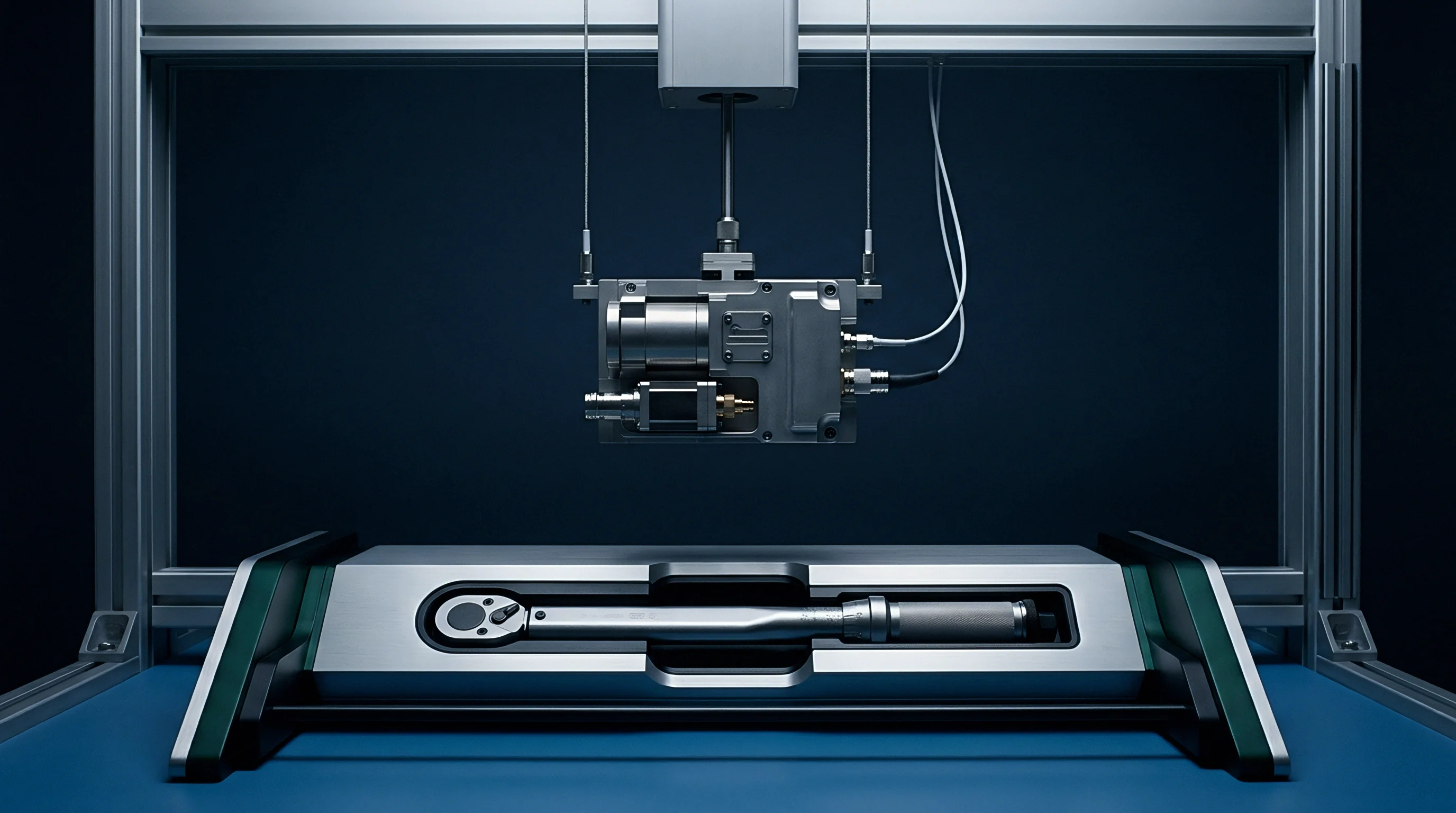
Physical Parasitics of Production Test Sockets
Pogo pins and spring-loaded contacts present inductive discontinuities to high-speed RF signals. Pogo pin inductance varies from 0.5 nanohenries to 2.5 nanohenries depending on pin length, spring compression, and internal plunger contact geometry. This inductance creates high-frequency reflection loops that distort return loss measurements beyond 6 GHz.
Socket bodies also introduce parasitic ground loop inductance when ground return pins sit too far from signal pins.
Mechanical wear alters pin surface geometry over execution runs. Gold plating wears off spring tips after five thousand insertions, exposing nickel underplating and copper alloys that oxidize upon exposure to atmospheric humidity. Increased contact resistance degrades insertion loss repeatability.
When contact resistance fluctuates by 200 milliohms between test insertions, the measured S21 phase varies unpredictably, rendering static mathematical offsets useless for yield validation.
Production test fixture design relies on identifying discrete parasitic failure modes prior to committing volume manufacturing lines:
- Pogo pin inductive peak creates artificial return loss spikes above 10 GHz when signal-to-ground pin spacing exceeds one millimeter.
- Substrate dielectric absorption attenuates high-frequency S21 magnitude across microstrip routing channels, masking true device output power.
- Contact tip oxidation increases contact resistance variance, destabilizing phase angle measurement repeatability across automated test runs.
- Launch pin solder bridging generates localized capacitive shunt drops that shift transmission line characteristic impedance below design limits.
- Ground plane cavity resonance introduces sharp absorption dips into insertion loss curves when shielding walls sit near planar conductors.
Assuming custom test fixture parasitics remain within nominal reference board specifications masks mechanical socket decay and ignores the mathematical necessity of continuous fixture characterization.

Deconvolution
Extracting device scattering matrices mathematically isolates true component behavior from test channel loading. Vector network analyzers measure the combined system matrix containing the lead-in fixture, the internal component, and the lead-out fixture. Matrix deconvolution calculates the inverse transmission parameters (T-parameters or ABCD matrices) of the fixture halves, multiplying them against the measured combined matrix to isolate the central S-parameter block.
Data files carry full two-port matrices. Converting measured S-parameters into cascading T-matrices enables linear algebraic division. The left lead-in fixture matrix inverse premultiplies the total measured matrix, and the right lead-out fixture matrix inverse postmultiplies the product.
Numerical stability during matrix inversion dictates the accuracy of de-embedded results. Phase errors corrupt de-embedded output files when high measurement noise occurs near impedance nulls.

Mathematical Principles of IEEE 370 De-Embedding
IEEE Standard 370-2020 governs electrical characterization of high-speed interconnects and fixture de-embedding up to 50 GHz. The standard establishes protocols for designing 2x Thru calibration structures. A 2x Thru structure consists of the complete lead-in test trace directly connected to the lead-out test trace, omitting the device landing pad.
Splitting the 2x Thru measurement at its geometric center yields the individual S-parameter matrices for the left half and right half fixtures.
Impedance peeling transforms frequency-domain S-parameter data into the time domain using inverse fast Fourier transforms. Calculating time-domain reflectometry step responses pinpoints exact physical locations of impedance discontinuities along the test channel. The IEEE 370 algorithm isolates the central fixture junction, models asymmetric manufacturing variations between fixture halves, and enforces mathematical causality and passivity on the calculated fixture models before performing matrix inversion.
Execution of IEEE 370 2x Thru de-embedding on an inline production test station follows a strict mathematical sequence:
- Measure full two-port Touchstone S2P data for the unpopulated 2x Thru PCB coupon across the complete frequency sweep range.
- Transform S-parameter data to the time domain using a bandpass impulse mathematical conversion to locate trace reflection peaks.
- Determine the physical center location of the 2x Thru trace by identifying the main transmission delay midpoint.
- Split the 2x Thru time-domain response into symmetric left-half and right-half error network models.
- Apply time-domain gating to remove unexpected residual reflections originating outside the defined launch and routing zones.
- Convert the gated time-domain model back to frequency-domain S-parameter matrices for both fixture halves.
- Enforce passivity enforcement algorithms to prevent S-parameter magnitudes from exceeding unity due to measurement noise.
- Convert left and right fixture S-parameters into ABCD transmission matrices for direct matrix inversion processing.
- Calculate the inverse of the left ABCD matrix and the inverse of the right ABCD matrix.
- Multiply the inverse left matrix by the measured DUT-in-fixture ABCD matrix, then multiply by the inverse right matrix to extract raw DUT performance.
- Convert the resulting DUT ABCD matrix back into standard Touchstone S2P format for automatic limit evaluation.

Time-Domain Gating and Automatic Fixture Removal
Time-domain gating applies a mathematical filter window to time-domain reflectometry sweeps, truncating reflections outside a designated physical window. Truncating signals beyond the launch connector eliminates reflections from cable interfaces and instrument ports. Applying gating requires setting window span and shape functions, such as minimum, normal, or maximum Kaiser-Bessel windows, to avoid introducing side-lobe ringing into the converted frequency-domain data.
Automatic Fixture Removal (AFR) utilizes 1x Thru or 1x Reflect structures when physical PCB space limits preclude layout of full 2x Thru structures. AFR uses time-domain gating to extract single-ended fixture models using open or short calibration standards. While 1x AFR reduces board area overhead on manufacturing test coupons, it exhibits higher sensitivity to substrate dielectric variations than 2x Thru algorithms.
Mathematical matrix inversion generates numerical noise when de-embedding highly reflective, non-50-ohm test channels.
IEEE Standard 370-2020 specifies maximum allowable fixture asymmetry of 0.5 dB magnitude and 5 degrees phase to prevent mathematical inversion singularities.
| Algorithm Method | Bandwidth Limit | Coupon Area Demand | Execution Overhead | Thermal Sensitivity |
|---|---|---|---|---|
| IEEE 370 2x Thru (2x-Thru) | 50 GHz | High (Full trace pair) | 120 ms per DUT | Low (Self-compensating) |
| Automatic Fixture Removal (1x-AFR) | 28 GHz | Low (Single launch) | 45 ms per DUT | Moderate (Requires lookup table) |
| Thru-Reflect-Line (TRL) | 110 GHz | Very High (Multiple lines) | 350 ms per DUT | High (Line length sensitive) |
| Time-Domain Gating (Single-Port) | 18 GHz | Zero (Uses DUT trace) | 15 ms per DUT | Extreme (Ringing artifacts) |
Factory test specifications must include an explicit clause stating: “De-embedding files shall be generated using IEEE 370 2x Thru algorithms applied to daily coupon sweeps; static s2p substitution is strictly prohibited.”


Rig
Automated production stations route raw microwave measurements through switching matrices, co-axial lines, and pneumatic actuators. Mechanical tolerances inside test nests dictate how reliably RF probes interface with printed circuit boards. Minor mechanical misalignments shift reference planes, introducing phase errors that bypass software de-embedding logic.
Uncorrected reflections degrade yield figures. Cable flexure during automated robotic pickup alters insertion phase, while thermal expansion inside enclosed manufacturing cells shifts microstrip electrical lengths over long production runs. Managing these physical variables requires strict hardware qualification protocols across contract manufacturing lines.

What Happens When Launch Pin Contact Shifts?
Lateral position deviations exceeding 50 micrometers shift signal pin contact points relative to ground vias on coplanar launch structures. Shifts in contact geometry alter localized shunt capacitance. The de-embedding matrix, derived from a centered pin reference layout, overcompensates or undercompensates for this localized capacitance.
The resulting de-embedded S11 sweep exhibits artificial ripple patterns that cause pass-fail yield instability.
Vertical probe force variation alters contact resistance and ground inductance. Low probe pressure creates micro-air gaps between ground pins and pad surfaces, introducing series inductance up to 800 picohenries. High probe pressure deforms landing pads, creating metallic micro-shavings that bridge RF signal lines to adjacent ground planes.
Automated test nests integrate load cell sensors to verify mechanical downforce on every actuation cycle.
Vector network analyzers on automated test lines experience S21 phase drift exceeding 1.8 degrees per degree Celsius without active thermal compensation.

Thermal Drift and Cable Phase Stability
Production environments experience ambient temperature changes driven by mechanical equipment heating and HVAC cycling. Phase-stable co-axial cables exhibit electrical length variations when internal fluoropolymer dielectrics expand or contract. Standard double-shielded RF cables shift phase by up to 0.5 degrees per meter per degree Celsius at 28 GHz.
Uncompensated phase shifts create virtual trace length errors in de-embedding algorithms.
Vector network analyzers drift during continuous operation. Internal synthesizer heating shifts source power output levels by up to 0.2 dB over an eight-hour operating window. Periodic recalibration resets analyzer baseline performance.
Standard Electronic Calibration (ECal) modules placed inside automated test cells perform automated re-calibration sequences at predefined time intervals, resetting VNA internal error terms without manual operator intervention.
| Error Source Origin | Magnitude Impact (S21) | Phase Uncertainty (S21) | Dominant Physical Cause | Mitigation Protocol |
|---|---|---|---|---|
| Cable Flexure Motion | ±0.12 dB | ±2.4 degrees | Mechanical robotic bending | Arm-arm armor sleeving |
| Contact Pin Compression | ±0.25 dB | ±4.1 degrees | Spring force variation | Inline load-cell monitoring |
| Thermal Ambient Drift | ±0.18 dB | ±3.6 degrees | Factory HVAC temperature cycles | Thermal-controlled nest cell |
| Substrate Dk Tolerance | ±0.30 dB | ±5.2 degrees | PCB batch dielectric variation | Per-batch coupon extraction |
| VNA Source Power Drift | ±0.05 dB | ±0.8 degrees | Internal amplifier heating | Automated ECal interval routines |
Hardware implementation scope for turn-key RF test cells mandates specific physical component configurations:
- Armored phase-stable cables preserve phase velocity calibration under continuous robotic arm movement.
- Pneumatic precision nests align landing pads within 15-micrometer position boundaries to prevent parasitic contact shifts.
- Automated ECal modules perform baseline VNA error corrections at scheduled four-hour manufacturing intervals.
- Inline micro-load sensors measure probe compression force to detect worn springs prior to RF contact failure.
- Integrated test coupons provide daily 2x Thru calibration verification channels directly on production panel margins.
Probes wear down long before Vector Network Analyzer calibration standards expire.

Audit
Auditing factory test execution ensures that calibration standards match real board stack-ups. Contract manufacturers operating under speed incentives occasionally bypass multi-step de-embedding sequences, substituting static S2P files collected during line setup weeks prior. Static files fail to reflect daily board dielectric changes or pin wear, producing false yield results.
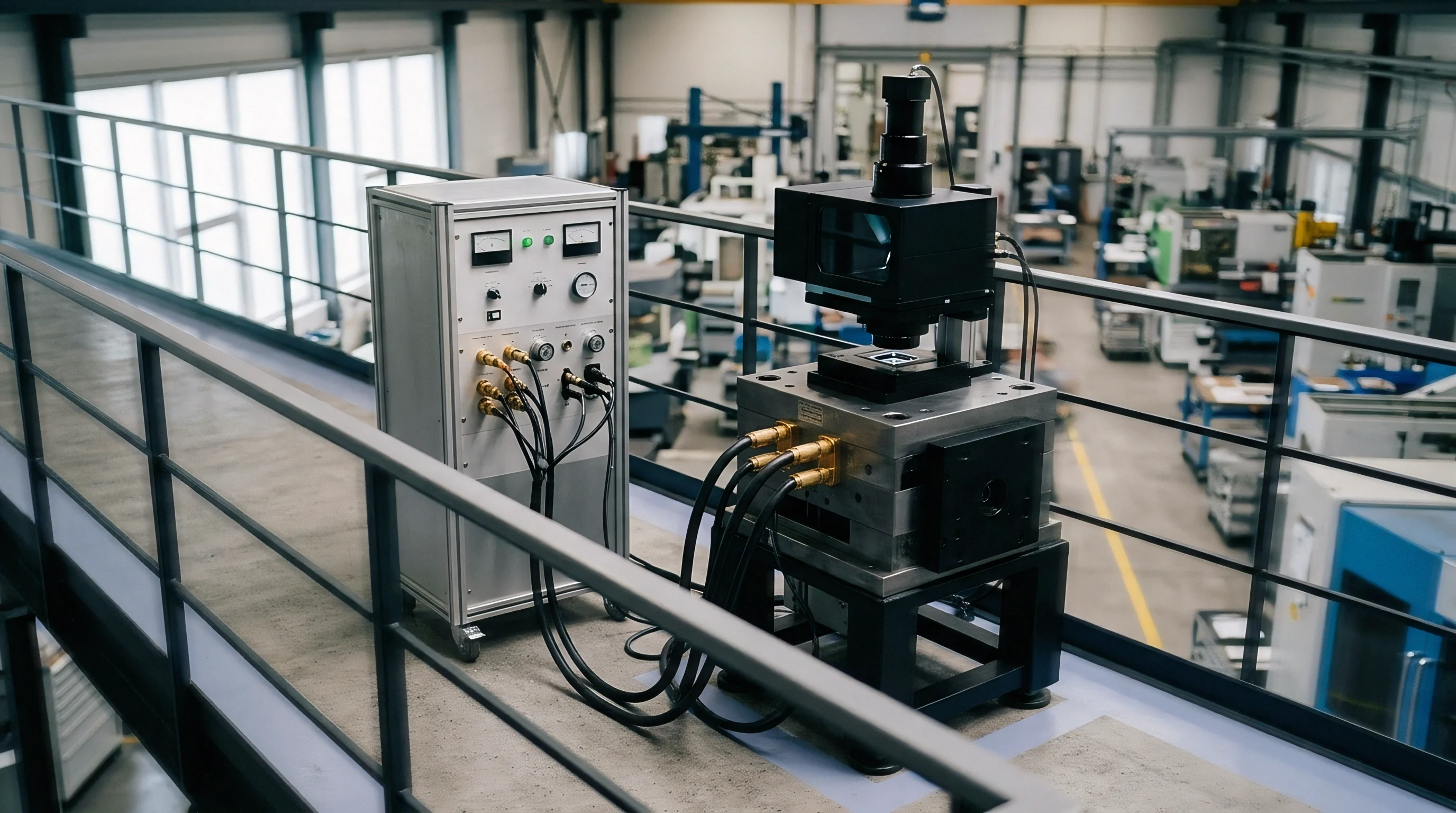
Audit procedures review automated test software logs, verifying raw and de-embedded Touchstone file generation timestamps. Algorithmic verification routines calculate causality and passivity metrics for extracted S-parameter matrices. De-embedded output files demonstrating S21 magnitude figures greater than 0 dB on passive devices indicate broken matrix inversion routines or corrupt baseline calibration files.
Verification of Touchstone S2P File Integrity
Touchstone file formats (v1.1 and v2.0) store multi-port network data in frequency-domain matrix format. Files contain header strings defining frequency units (Hz, MHz, GHz), parameter type (S, Y, Z, H), and data format (MA for magnitude-angle, DB for dB-angle, RI for real-imaginary). Parsing errors occur when contract manufacturing software misinterprets magnitude-angle formats as real-imaginary data pairs, causing catastrophic phase calculation failures in automated limit checking.
Automated file validation checks verify matrix symmetry on passive structures. Reciprocal passive networks demand that S12 equals S21 within predefined tolerance margins. Differences exceeding 0.3 dB between S12 and S21 indicate measurement channel non-linearity, ground loop corruption, or improper VNA receiver calibration.
Passivity checks confirm that eigenvalues of the S-parameter matrix remain bounded by unity across all measured frequency points.

Production Line Quality Control Protocols
On-line audit scripts evaluate daily test performance by comparing coupon de-embedding outputs against baseline gold standards. Gold standards consist of precision-machined copper-on-quartz verification substrates with known, NIST-traceable S-parameters. Automated nest control software blocks production execution whenever gold standard verification runs drift beyond defined error bounds.
Configuration management protocols tie software de-embedding routines to specific product board revisions. Changes in PCB laminate supplier, solder mask thickness, or copper foil roughness invalidate existing de-embedding lookup tables. Contract manufacturing quality teams maintain clear part-change notification (PCN) boundaries that mandate fixture re-characterization whenever substrate suppliers change.
Evaluations of contract manufacturing high-frequency test lines use a structured operational verification matrix:
- Header format validation checks Touchstone S2P files for correct unit declaration and data format structure before limits processing.
- Passivity violation limits flag any de-embedded passive component demonstrating S21 or S11 magnitude responses above 1.0.
- Causality enforcement rules verify time-domain step responses to confirm signal arrival occurs after physical propagation delay.
- Reciprocity symmetry checks measure S12 versus S21 divergence to identify non-linear pin contact behavior.
- Golden unit verification sweeps compare daily line setup outputs against certified physical standards prior to running production lots.
Contract manufacturing facilities often manage high product turnover by reusing single de-embedding matrices across multiple PCB trace layouts, leaving buyers to determine how many out-of-spec modules passed testing before the discrepancy was discovered.


Ledger
Commercial contracts dictate whether test yield drops caused by calibration error belong to the factory or the OEM. Yield losses originating from un-de-embedded fixture parasitics create friction between engineering teams and purchasing managers. When a contract manufacturer quotes high product assembly yields but experiences high test scrap due to improper de-embedding, financial responsibility hinges on contract boundary definitions.
Non-recurring engineering (NRE) costs cover custom fixture design, precision coupon fabrication, and automated software integration. Scope assignments clarify who owns the custom de-embedding algorithms andTouchstone calibration tables. OEM ownership of all calibration files, coupon designs, and automated test software source code prevents vendor lock-in and allows seamless transfer of assembly lines to alternative manufacturing partners.
Non-Recurring Engineering Costs for Custom Test Hardware
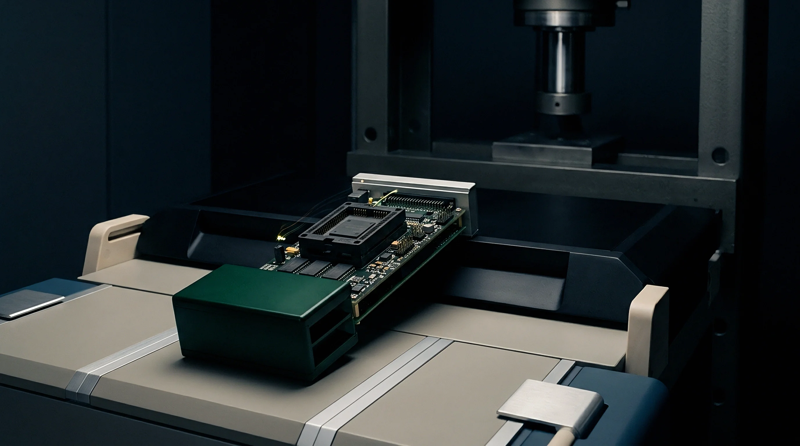
Developing dedicated high-frequency de-embedding infrastructure demands upfront capital allocation. Designing high-precision 2x Thru validation coupons on target PCB laminates adds tooling charges to initial prototype runs. Automated RF test nest engineering costs include high-durability pogo sockets, precision alignment slides, and customized VNA control software driver code.
Amortizing NRE costs over planned unit production volumes reveals the true cost of high-frequency testing. Skipping dedicated de-embedding coupon integration reduces initial tooling invoices by several thousand dollars. That upfront saving increases long-term operational expense by raising false rejection scrap rates on final assembly lines.
Factory test software that strips fixture de-embedding tables to accelerate production line cycle time transfers test fixture artifacts directly into customer return line failure rates.
| Implementation Strategy | Upfront NRE Investment | Unit Cycle Time Overhead | Expected Scrap Rate | Break-Even Volume Point |
|---|---|---|---|---|
| Full IEEE 370 Automated Coupon De-Embedding | $45,000 | +180 ms per unit | 0.2% (False fails eliminated) | 35,000 units |
| Static S2P File Matrix Substitution | $12,000 | +15 ms per unit | 2.8% (Fixture drift uncorrected) | 120,000 units |
| Manual Recalibration Routine (Hourly) | $5,000 | +45 sec per hour block | 1.5% (Operator variance) | 15,000 units |
| No De-Embedding (Raw Measurement Bounds) | $0 | 0 ms | 8.5% (Wide guard-bands applied) | Never breaks even |

Yield Scrap Allocation and Financial Liability
Statements of Work must assign financial responsibility for scrap generated by invalid test execution. If factory line operators run production using expired calibration tables or corrupted de-embedding files, the resulting rejected units represent factory operational scrap rather than genuine component failure. Contract clauses define target yield agreements based strictly on valid, mathematically verified de-embedded S-parameter data.
Supply agreements specify scrap credit thresholds. When test scrap exceeds agreed baseline percentages due to uncorrected fixture drift, contract manufacturers absorb the material costs of destroyed components. Clear financial liability rules enforce daily execution of IEEE 370 calibration verification sequences across all active assembly shifts.
Failing to embed rigorous de-embedding standards within turnkey manufacturing contracts forces original equipment manufacturers to absorb high scrap expenses caused by uncorrected fixture loss and false component failures.