Characterizing Contact Surface Oxidation Dynamics in Modular RF Interconnects
Surface oxidation at RF contact interfaces increases skin-effect insertion loss and link margin erosion, requiring controlled normal force and plating standards.

Film
Surface metallurgy controls the initial signal path in sub-miniature coaxial and board-to-board contacts. When two metallic conductors meet inside an RF interconnect, actual mechanical contact occurs only at microscopic high points called asperities, making effective electrical contact area a tiny fraction of the total geometric surface. At these localized contact spots, raw substrate metals face immediate exposure to oxygen, ambient humidity, and airborne contaminants.
Non-precious base metals such as copper, brass, and beryllium copper form native oxide layers within seconds of air exposure. Nickel underlayers, applied beneath thin gold electroplating to prevent copper migration, form a passivating nickel oxide film through microscopic pores in the noble top layer. High-frequency electrical current does not pass uniformly through the entire cross-section of the mating pin; instead, high-frequency electromagnetic fields force the current into a thin surface layer defined by skin depth.
Native copper oxides, primarily cuprous oxide and cupric oxide, act as semiconductor barriers across the contact interface. Nickel oxidizes rapidly in ambient air. When oxide growth reaches a thickness between two and ten nanometers, direct metallic conduction ceases.
Electrons must either tunnel quantum-mechanically through the oxide dielectric layer or rupture the film via dielectric breakdown. Quantum tunneling occurs efficiently only across oxide films thinner than two nanometers, yielding a predictable tunneling resistance. Once oxide growth exceeds five nanometers, interfacial resistance increases by several orders of magnitude.
The application of mechanical contact normal force squeezes the mating surfaces, fracturing brittle oxide layers and forcing fresh metal through the fissures to form direct metal-to-metal bridges. Lower contact normal force leaves intact oxide films trapped between asperities, elevating initial contact resistance from single-digit milliohms to tens of ohms.
Oxide Conduction Mechanics and Fritting Breakdown
Current transport across un-mated metallic junctions depends on dielectric thickness. When an applied voltage across a thin oxide film exceeds the dielectric strength of the oxide layer, electrical breakdown occurs. This voltage-induced film rupture, termed fritting, forms tiny molten metal channels through the oxide barrier.
B-fritting occurs when the voltage across the contact interface reaches the melting voltage of the contact metal, typically 0.3 to 0.4 volts for copper and nickel systems. B-fritting expands existing conductive metallic bridges, reducing localized contact resistance. A-fritting occurs at higher open-circuit voltages when an insulating film breaks down entirely to create new conductive channels.
In low-power RF applications where signal voltages remain below ten millivolts, the operating signal level lacks the electrical potential necessary to induce fritting. Micro-power RF interconnects operating in sensor nodes or cellular handsets must overcome native contact resistance without relying on signal-driven dielectric breakdown.
Contact resistance instability in micro-power RF links occurs when ambient signal voltages remain below the ten-millivolt threshold required for oxide fritting breakdown.
Fritting phenomena introduce extreme signal non-linearity into the interconnect. Because fritting depends on the instantaneous voltage waveform, high-amplitude transmit bursts dynamically collapse the contact impedance, whereas low-amplitude receive signals encounter high insulating barrier resistance. This amplitude-dependent impedance shift distorts the RF waveform, generating spurious intermodulation products.
The operational consequence manifests as degraded receiver sensitivity and intermittent packet dropouts in low-noise amplifier front ends. RF interfaces utilizing non-noble metal contacts or thin flash gold over nickel remain highly susceptible to fritting-induced signal instability when deployed in harsh operating environments.
Skin Depth Redistribution at Microwave Frequencies
Alternating current at two gigahertz concentrates within a surface layer under two micrometers deep. The mathematical expression for skin depth governs the distribution of RF current density from the outer boundary into the interior of the conductor:
Skin Depth Formula ~ delta = sqrt( rho / ( pi freq mu ) )
In this relationship, rho represents material electrical resistivity in ohm-meters, freq denotes signal frequency in hertz, and mu represents absolute magnetic permeability in henries per meter. At sub-gigahertz frequencies, such as 868 MHz or 915 MHz LoRaWAN allocations, skin depth in gold is approximately 2.6 micrometers. At 2.4 GHz Wi-Fi frequencies, skin depth drops to 1.5 micrometers.
At 5.8 GHz, skin depth shrinks to less than 1.0 micrometer. In 24 GHz to 39 GHz 5G millimeter-wave interconnects, skin depth drops below 0.4 micrometers. Signal loss scales with frequency.
When surface oxidation forces current through a high-resistivity oxide shell or through an oxidized nickel underlayer exposed by porous gold plating, the effective series resistance of the RF transmission line rises dramatically.
Skin depth shrinkage concentrates current flow directly inside the damaged outer surface layer. If a gold flash plating layer of 0.05 micrometers wears away, the high-frequency current shifts entirely into the underlying nickel oxide and copper substrate layers. Because nickel possesses a magnetic permeability significantly higher than copper or gold, the skin depth within a nickel underlayer collapses to a fraction of its non-magnetic value, exacerbating conductor attenuation.
RF insertion loss increases not merely from the DC contact resistance rise, but from the increased attenuation coefficient of the distorted electromagnetic wave propagating along the oxidized surface layer. Connectors designed for microwave applications require stable surface conductivity to maintain specified return loss and insertion loss parameters over their operating lifespan.
Mechanical wiping action during connector mating can shear away surface oxides and temporarily restore original contact resistance figures, though initial signal degradation still occurs prior to full engagement.


Wear
Micro-scale movements between mated contact points destroy protective surface treatments over time. Thermal expansion variances across printed circuit boards force continuous relative displacement at connector pins. When an RF module mounted on a host board undergoes temperature cycling during power-up and power-down sequences, differential thermal expansion causes relative motion between the plug and receptacle contacts.
Mechanical vibration from industrial machinery or vehicle operation induces similar cyclic micro-displacement. This relative movement, ranging from 1 to 100 micrometers in amplitude, causes fretting. Fretting breaks the noble metal plating, exposes underlying base metals to atmospheric oxygen, and traps insulating oxide debris within the contact zone.
The accumulating debris isolates the metallic asperities, causing contact resistance to fluctuate wildly under mechanical disturbance.
Contact normal force defines the mechanical pressure driving two mating contact surfaces together. Initial spring design provides sufficient force to establish low contact resistance. Over extended exposure to elevated temperatures, spring materials like beryllium copper and phosphor bronze experience stress relaxation.
Atoms inside the metal lattice rearrange to relieve internal stress, reducing the spring force exerted by the contact beam. As normal force drops below critical thresholds—typically 0.3 to 0.5 newtons for precision RF connectors—the mechanical wiping action during micro-motion becomes ineffective at clearing oxidation products. The reduced contact pressure allows oxide layers to build up unchecked inside the contact zone, driving severe RF signal degradation and impedance mismatching.
Fretting Corrosion and Interfacial Micro-Motion
Cyclic mechanical displacement converts metallic contact zones into layered oxide wear tracks. During the initial motion cycles, mating asperities shear the thin gold surface layer. Hard gold coatings containing small quantities of cobalt or nickel resist shear better than soft pure gold, but both suffer wear under persistent high-cycle fretting.
Once wear penetrates the gold layer, the underlying nickel flash is exposed to ambient air. Subsequent movement breaks the brittle nickel oxide layer, producing fine, highly abrasive nickel oxide particles. These oxide particles become trapped within the localized contact interface, acting as an abrasive slurry that accelerates wear on remaining intact metal areas.
Interfacial wear mechanics progress through distinct physical stages:
- Metallic Shearing Phase ~ Primary asperities shear under applied contact normal force, causing initial transfer of soft gold plating across the mating interface without immediate electrical performance loss.
- Underlayer Exposure Stage ~ Continuous micro-displacement wears through the noble top plating, exposing the passivating nickel underlayer to ambient atmospheric oxygen.
- Debris Accumulation Process ~ Repeated mechanical cracking of newly formed nickel oxides generates loose, insulating oxide particles that lodge within the electrical contact path.
- Impedance Instability Phase ~ Trapped oxide debris isolates remaining metallic contact points, causing rapid spikes in localized contact resistance and intermittent RF signal loss.
Accumulated wear debris alters the geometric profile of the contact interface. The insulating oxide particles force the metallic spring contact away from the mating pin, creating a physical gap filled with mixed metallic oxides and air voids. This structural separation changes the capacitance and inductance of the connector junction.
At gigahertz frequencies, this geometric alteration creates a localized impedance discontinuity, driving up the Voltage Standing Wave Ratio (VSWR) and reflecting transmit power back into the output power amplifier.

Passive Intermodulation Generation at Corroded Contacts
Non-linear resistance across oxidized metal junctions transforms high-power transmit signals into parasitic intermodulation products. Passive Intermodulation (PIM) occurs when two high-power RF carriers pass through a non-linear junction within a passive component. An oxidized contact interface acts as a metal-insulator-metal diode array.
Equation models demonstrate that the current-voltage relationship across an oxide film contains exponential and cubic terms, transforming a linear resistive contact into a frequency-mixing element. When transmit frequencies f1 and f2 pass through an oxidized interconnect, third-order intermodulation products generated at 2 f1 – f2 and 2 f2 – f1 fall directly into adjacent receive channels.
| Plating System | Initial Contact Force (N) | Force After 1000h at 105C (N) | Fretting Cycle Resistance (Spike Threshold) | 3rd Order PIM at 1.8 GHz (dBc) |
|---|---|---|---|---|
| Flash Gold (0.05 µm) over Nickel | 0.45 | 0.28 | 1,500 cycles | -85 |
| Hard Gold (0.76 µm) over Nickel | 0.50 | 0.38 | 25,000 cycles | -115 |
| Silver (2.5 µm) over Copper | 0.60 | 0.42 | 8,000 cycles | -125 |
| Tin-Lead (3.0 µm) over Brass | 1.20 | 0.55 | 400 cycles | -65 |
Third-order PIM levels of -85 dBc or worse destroy the sensitivity of modern multi-carrier cellular base stations and multi-band IoT gateways. A high power transmit carrier of +43 dBm passing through an oxidized board-to-board connector generates PIM signals at -42 dBm. This spurious power exceeds the noise floor of a standard LTE or 5G NR receiver by more than 60 dB, completely desensitizing the receive channel.
PIM generation worsens significantly as fretting wear accumulates. Connectors maintaining low initial static resistance can exhibit severe dynamic PIM generation when subjected to ambient vibration profiles.
Gold yields under clamping force to form a tight mechanical contact.


Atmosphere
Ambient chemical agents penetrate thin metallic plating through sub-micron structural voids. Electroplated gold coatings inherently display pinhole porosity when deposited at thicknesses below 0.76 micrometers. Pores in the gold layer expose the underlying nickel or copper directly to atmospheric gases.
In industrial environments, gaseous pollutants including hydrogen sulfide, sulfur dioxide, chlorine, and nitrogen dioxide react with the exposed substrate metals. Substrate corrosion products migrate outward through the porosity network via capillary action and surface diffusion, forming expanding mounds of insulating tarnish on top of the noble gold contact surface.
Galvanic corrosion amplifies oxidation kinetics when dissimilar metals interact in the presence of an electrolyte. Gold possesses an electrochemical potential of +1.50 volts relative to a standard hydrogen electrode, while nickel sits at -0.25 volts and copper at +0.34 volts. When atmospheric moisture condenses within plating pores to form a microscopic electrolyte film, a powerful galvanic cell forms between the gold top layer and the underlying nickel or copper substrate.
The base metal acts as a sacrificial anode, dissolving rapidly and producing bulky metallic hydroxides and oxides. These corrosion products spill out of the pore structures, coating the surrounding gold surface in a highly resistive layer that elevates high-frequency insertion loss.
Galvanic Reaction Channels in Porous Gold Plating
Substrate copper migrates through thin gold coatings when humidity exceeds sixty percent. Under conditions of high relative humidity, liquid water films several monolayers thick condense on metallic surfaces. Dissolved atmospheric carbon dioxide, sulfur compounds, and airborne chloride salts turn this condensed water layer into a conductive electrolyte.
The gold-nickel galvanic couple drives rapid anodic dissolution of the nickel underlayer. Nickel ions react with hydroxyl ions in the condensed electrolyte to form nickel hydroxide, which subsequently dehydrates into insulating nickel oxide.
The rate of porous gold tarnish growth depends heavily on gold plating thickness and deposition chemistry. Electroplated soft gold exhibits higher porosity than cobalt-hardened gold at equivalent thicknesses. Standard test protocols utilize Flowers of Sulfur (FOS) exposure or mixed flowing gas testing to quantify porosity-driven atmospheric corrosion rates.
Plating porosity metrics demonstrate an exponential relationship between plating thickness and pore density:
Porosity Scaling Law ~ Pore_Density = A exp( -b Plating_Thickness )
Where Plating_Thickness represents gold layer thickness in micrometers, and A and b represent empirical deposition parameters. At a flash gold thickness of 0.05 micrometers, pore density often exceeds 50 pores per square millimeter. Increasing gold plating thickness to 0.76 micrometers reduces pore density to near zero, effectively closing the galvanic reaction channels and protecting the underlying nickel barrier from atmospheric exposure.
Sulfur Tarnish Mechanics in Silver-Plated Interfaces
Airborne hydrogen sulfide reacts rapidly with silver matrix elements to create non-conductive sulfide barriers. Silver plating offers exceptional initial electrical conductivity and low cost compared to gold, making it attractive for high-power sub-GHz RF interconnects and filter housings. However, silver lacks noble chemical stability in environments containing reduced sulfur gases.
Hydrogen sulfide gas at concentration levels as low as one part per billion reacts with silver to form silver sulfide tarnish:
Silver Sulfide Reaction ~ 2 Ag + H2S + 0.5 O2 -> Ag2S + H2O
Silver sulfide is a black, poorly conductive semiconductor with a high bandgap energy. Unlike copper oxides, which can be partially fractured by mechanical wiping, silver sulfide exhibits high ductility and tends to smear across the contact interface under mechanical contact pressure. The resulting film increases low-level contact resistance from less than one milliohm to several hundred milliohms.
Plating porosity standards require zero exposed nickel substrate under ten-times optical magnification after twenty-four hours of exposure to nitric acid vapors per ASTM B735 testing protocols.
Temperature accelerates sulfur tarnish kinetics. In automotive engine compartments or outdoor industrial deployments, elevated ambient temperatures double the tarnish reaction rate for every ten-degree Celsius rise. The growing silver sulfide film squeezes the skin-depth conduction layer, pushing high-frequency RF currents into the highly resistive sulfide barrier.
At 5.8 GHz, a silver sulfide layer thickness of just 100 nanometers increases RF insertion loss by up to 0.4 dB per contact interface. In a modular system containing multiple board-to-board and antenna interconnects, cumulative insertion loss quickly consumes the entire link budget allocation.
Failing to account for atmospheric porosity creep in thin-gold interconnects results in unpredicted field failures, requiring costly on-site module replacements and total product recalls.

Gauge
Precision measurement of contact degradation demands strict electrical limits during bench evaluation. Standard ohmmeter measurements apply open-circuit voltages ranging from two to ten volts. These voltage levels break down delicate native oxide films through fritting, producing false low-resistance readings that mask true surface degradation.
Accurate characterization of contact oxidation requires dry-circuit testing protocols. Dry circuit testing limits the open-circuit voltage applied to the test sample to twenty millivolts or less, ensuring that the electrical test signal does not alter the physical or chemical state of the surface oxide films under evaluation.
Low-Level Contact Resistance (LLCR) testing utilizes a four-wire Kelvin measurement configuration. Two leads supply a controlled test current, while two independent sensing leads measure the voltage drop directly across the contact interface. By isolating the measurement circuit from lead wire resistance and instrument terminal resistance, four-wire LLCR techniques resolve contact resistance changes as small as ten micro-ohms.
Evaluating contact performance over time requires combining LLCR dry-circuit measurements with environmental stress cycling, such as thermal shock, damp heat steady-state, and random vibration profiling inside an environmental test chamber.
How Does Dry Circuit Testing Isolate Interface Degradation?
Voltage levels above twenty millivolts punch through delicate oxide films and mask true contact degradation. The strict twenty-millivolt open-circuit ceiling mandated by EIA-364-23 ensures that the electric field strength across thin interfacial oxides remains well below the dielectric breakdown threshold of 10^6 volts per centimeter. Current levels are limited to a maximum of one hundred milliamperes to prevent localized Joule heating at microscopic asperities.
Localized heating above fifty degrees Celsius causes thermal relaxation of contact material and thermal expansion that artificially alters the contact area during measurement.
Standard procedures for an LLCR measurement sequence involve the following steps:
- Mount the RF interconnect sample into a zero-strain four-wire Kelvin test fixture attached to a calibrated micro-ohmmeter.
- Set the test instrument open-circuit voltage limit to twenty millivolts peak-to-peak AC or direct DC voltage.
- Set the source current limit to one hundred milliamperes maximum.
- Record the initial baseline dry-circuit contact resistance at ambient room conditions across twenty distinct sample pairs.
- Transfer the test assembly into an environmental cycling chamber configured for high-temperature aging or mixed flowing gas exposure.
- Perform in-situ four-wire resistance measurements at specified thermal intervals, logging resistance drift with micro-ohm precision.
- Extract the test samples upon test completion and calculate total contact resistance delta against initial baseline figures.
Dry-circuit measurements provide the pure DC contact resistance of the interface. However, translating DC resistance changes into RF insertion loss and return loss degradation requires high-frequency S-parameter characterization across the operational band of the radio module.
Insertion Loss and Return Loss Tracking via Vector Network Analysis
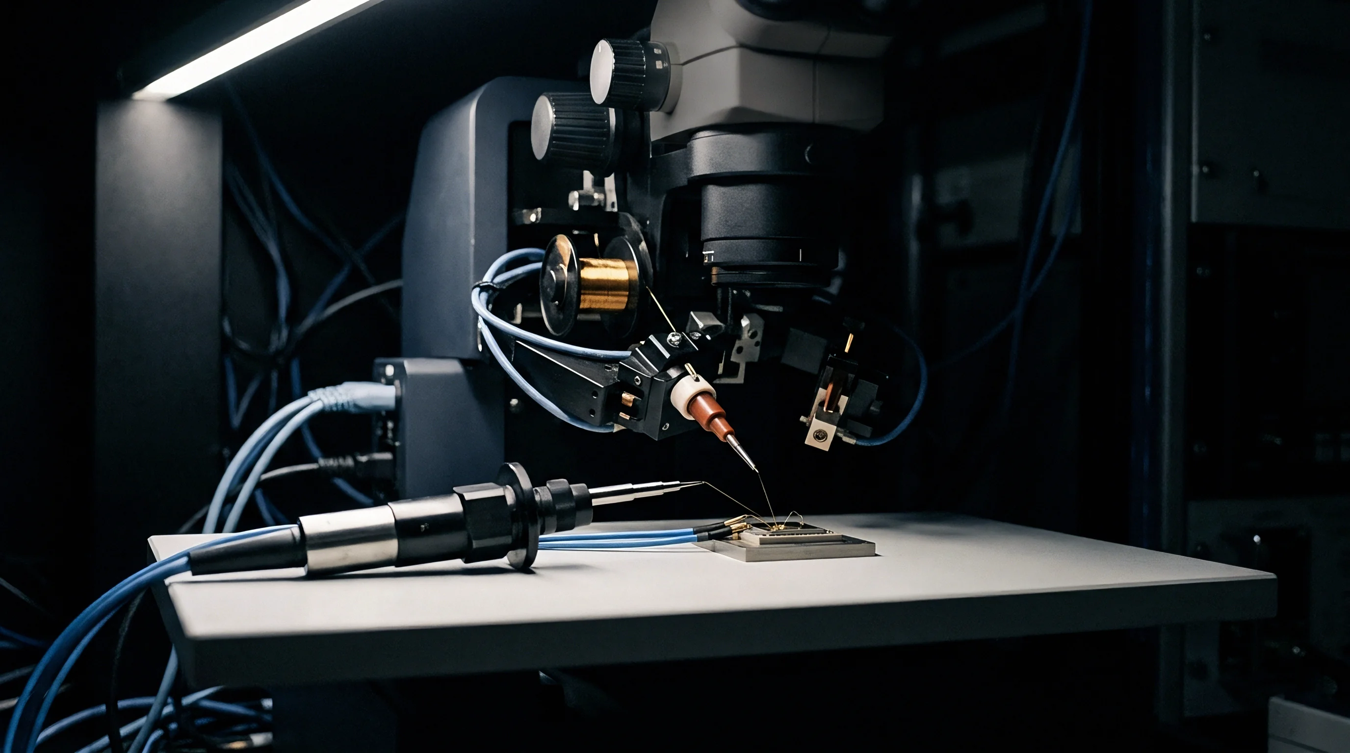
High-frequency signal degradation manifests as localized impedance mismatches across damaged contact zones. A Vector Network Analyzer (VNA) measures scattering parameters (S-parameters) to quantify how an oxidized interconnect alters RF signal propagation. S21 represents the forward transmission coefficient, defining insertion loss through the interconnect.
S11 represents the input reflection coefficient, defining return loss. As surface oxidation increases DC contact resistance, the high-frequency contact impedance transforms from a low-loss series resistance into a complex impedance consisting of increased series resistance in parallel with localized interface capacitance.
To isolate contact interface attenuation from printed circuit board trace loss, test engineers utilize De-embedding techniques such as Thru-Reflect-Line (TRL) or 2-Port Series-Thru calibration. Once trace losses are removed, changes in S21 accurately reflect oxidation-induced surface resistance changes. Consider a 50-ohm RF transmission line containing a single contact interface.
The relationship between interface contact resistance increase (delta_R) and RF insertion loss increase (delta_IL) can be calculated using transmission line theory:
RF Insertion Loss Delta Equation ~ delta_IL_dB = 20 log10( 1 + ( delta_R / ( 2 Z0 ) ) )
Where Z0 represents the characteristic impedance of 50 ohms. For a modest contact resistance increase of 1.0 ohm across a heavily oxidized interface, the theoretical DC insertion loss increase is calculated as:
delta_IL_dB = 20 log10( 1 + ( 1.0 / 100 ) ) = 20 log10( 1.01 ) = 0.086 dB
At microwave frequencies, skin depth effects elevate the Effective RF Resistance (R_rf) far above the DC resistance value. Due to skin effect and current concentration within surface oxide layers, R_rf at 5.8 GHz can exceed the DC contact resistance by a factor of 5 to 10. Assuming an effective high-frequency contact resistance increase of 5.0 ohms due to skin-depth current redistribution through an oxidized layer, the resulting RF insertion loss increase becomes:
delta_IL_dB = 20 log10( 1 + ( 5.0 / 100 ) ) = 20 log10( 1.05 ) = 0.424 dB
| Test Profile | Standard Standard Reference | Test Parameters | Pass/Fail LLCR Delta Ceiling | Max Permissible S21 Delta at 5.8 GHz |
|---|---|---|---|---|
| Thermal Shock | EIA-364-32 Method A | -55C to +105C, 100 cycles, 30 min dwell | +10 milliohms | 0.15 dB |
| Humidity Temperature Cycling | EIA-364-31 Method IV | 25C to 65C, 90-95% RH, 10 days | +15 milliohms | 0.20 dB |
| Mixed Flowing Gas (MFG) | EIA-364-65 Class IIA | H2S, NO2, Cl2, SO2, 14 days exposure | +20 milliohms | 0.30 dB |
| Vibration with Thermal Aging | EIA-364-28 Condition V | 10 to 2000 Hz, 15G peak, 105C, 8 hrs/axis | +10 milliohms | 0.15 dB |
A multi-contact board-to-board RF connector array containing four signal paths subjected to thermal shock cycling can accumulate over 1.6 dB of total insertion loss degradation across the module interface. Link margin absorbs interface attenuation. In long-range sub-GHz LoRaWAN links operating near receiver sensitivity limits, or high-throughput Wi-Fi 6E links utilizing 4096-QAM constellations, a 1.6 dB signal loss drops data rates or collapses maximum achievable range by up to twenty percent.
Contractual procurement specifications governing qualification testing explicitly demand: The vendor shall certify compliance with EIA-364-23 dry-circuit testing, guaranteeing low-level contact resistance drift remains below ten milliohms after exposure to ten-day mixed flowing gas profile Class IIA.

Allowance
Commercial specification sheets often obscure long-term environmental degradation behind ideal initial contact resistance figures. Module datasheets list fresh, un-mated contact resistance numbers measured under ideal laboratory conditions, typically quoting 10 to 20 milliohms maximum. These initial figures reflect pristine, oxide-free surfaces.
Sourcing practices require writing environmental aging requirements directly into supplier master service agreements to ensure field reliability. Purchasing cheap flash-gold connectors saves pennies on bill-of-materials costs upfront while creating massive warranty liabilities when field units fail due to fretting corrosion and surface tarnish.
Link budget calculations must allocate a dedicated hardware aging margin to absorb interconnect surface oxidation over product service life. Standard link budget practice accounts for path loss, fading, antenna gain, and noise figures, but frequently omits contact degradation. Designing a 0.5 dB to 1.0 dB interconnect attenuation allowance into the system link margin prevents premature field link failures.
Specifying higher-grade contact plating systems directly addresses oxidation kinetics at the source, extending component operating life across industrial and outdoor deployment environments.

Plating Thickness Economics and Life-Cycle Trade-Offs
Specifying thirty micro-inches of hard gold increases connector unit cost while extending field service life. Hard gold resists mechanical wear. Hard gold plating deposited at 0.76 micrometers (30 micro-inches) over 1.27 micrometers (50 micro-inches) of nickel provides an effective barrier against atmospheric sulfur and humidity ingress.
Thin flash gold plating, deposited at 0.05 micrometers (2 micro-inches) or less, contains high pinhole density and wears away within five to ten mating cycles. While flash-gold connectors cost 30 to 40 percent less per unit than hard-gold equivalents, their rapid degradation in outdoor or high-vibration applications renders them unsuitable for high-reliability modular RF systems.
Sourcing strategies for robust RF interconnect procurement prioritize key technical clauses:
- Plating Material Composition ~ Hard gold electroplating alloyed with 0.1 percent cobalt to increase mechanical hardness and resist fretting shear during thermal expansion cycles.
- Underlayer Barrier Thickness ~ Sulfamate nickel underplate deposited at a minimum thickness of 1.27 micrometers to block copper substrate diffusion toward the top interface layer.
- Porosity Certification Limits ~ Mandatory nitric acid vapor testing per ASTM B735 proving zero pinhole defects per square millimeter across critical contact mating zones.
- Contact Normal Force Minimums ~ Guarantees of initial contact force exceeding 0.50 newtons, with maximum allowable stress relaxation under 25 percent after 1000 hours at 105 degrees Celsius.
- Mating Cycle Durability Ceilings ~ Certified performance sustaining 500 mating cycles without exposing underlying nickel or exceeding a 10-milliohm dry-circuit resistance increase.
Balancing plating costs against lifetime operational expenses requires evaluating the total landed cost of field failures. A commercial gateway deployment utilizing cheap flash-gold modular antenna connectors may suffer a ten percent annual failure rate in humid coastal environments. The labor cost of dispatching a service technician to replace a failed radio module far outweighs the initial thirty-cent component savings achieved by selecting lower-grade RF interconnects.
Designing a dedicated one-decibel attenuation allowance into the RF link margin absorbs interconnect oxidation drift over a ten-year operational lifespan without triggering packet loss.
Will future multi-GHz modular radio standards adopt non-contact capacitive or inductive RF interfaces to eliminate mechanical contact oxidation entirely, or will advancements in synthetic lubricant barriers extend physical contact viability?