Dynamic Load Pull Phase Shifts Altering Power Amplifier Conduction Waveforms in Miniaturized Radios
Dynamic antenna impedance phase shifts alter power amplifier conduction angles, elevating peak drain voltages and causing adjacent channel leakage failures.


Knee
Transistor operating points inside compact radio modules distort the moment the load reflection coefficient rotates across the complex impedance plane. In miniaturized radios operating across the 868 MHz, 2.4 GHz, or 5.8 GHz bands, physical space constraints eliminate the isolation margins traditional base station designs rely upon. When antenna radiation resistance shifts due to environmental detuning, the terminal load seen by the power amplifier pulls away from the nominal 50-ohm reference.
The resulting reflection coefficient, defined by its magnitude and phase angle, forces the RF load line to wander across the transistor output characteristics during operation.

Phase Rotation across Complex Load Vectors
Antenna impedance shifts pull output terminal conditions along a constant voltage standing wave circle on the Smith chart. While standing wave magnitude determines total reflected power, the phase angle dictates the physical alignment of instantaneous voltage and current waveforms at the semiconductor drain node. At phase angles where the load vector turns strongly inductive, drain voltage swings expand well beyond the nominal direct-current supply rail.
Capacitive phase angles, by contrast, compress the voltage swing, forcing peak current conduction to occur while drain voltage remains high.
Voltage waveform expansion under inductive load phases presents severe reliability risks for sub-micron silicon processes. In a 3.3-volt Complementary Metal-Oxide-Semiconductor or Gallium Arsenide power stage, a 3:1 voltage standing wave ratio with an inductive phase alignment drives peak drain voltage spikes beyond 9 volts. Gate-oxide stress accelerates under these localized high-field conditions, causing microscopic breakdown and altering channel threshold voltages over extended operating periods.
A 3:1 standing wave ratio at a phase angle of 135 degrees elevates peak drain voltage to 2.8 times the nominal supply voltage in a 2.4 GHz Class AB power stage.

Drain Saturation and Knee Line Clipping
RF output devices subjected to reactive load shifts compress signals early when instantaneous collector or drain potentials drop below semiconductor channel boundary limits. The knee voltage marks the boundary between the linear active region and the ohmic saturation region of the field-effect transistor. When dynamic load pull phase shifts drive the instantaneous load line into this low-voltage boundary during peak drive conditions, the drain voltage waveform flattens sharply against the knee line.
Knee line clipping truncates the upper envelope of the amplified signal, generating severe odd-order intermodulation distortion. Inductive load phase vectors cause voltage to lead current, opening wide elliptical trajectories on the current-voltage plane. As these trajectories cross the knee boundary, the current waveform undergoes asymmetric flattening.
Fundamental output power drops while higher-order harmonic energy increases, altering the spectral purity delivered to the antenna feed line.
| Phase Angle (°) | Peak Drain Voltage (V) | Peak Drain Current (mA) | Conduction Angle (°) | Power Added Efficiency (%) | Peak Output Power (dBm) |
|---|---|---|---|---|---|
| 0 | 6.4 | 210 | 200 | 42.5 | 24.1 |
| 45 | 7.2 | 185 | 185 | 38.1 | 23.5 |
| 90 | 8.6 | 150 | 170 | 31.0 | 22.2 |
| 135 | 9.2 | 135 | 160 | 26.4 | 21.0 |
| 180 | 6.1 | 240 | 225 | 36.8 | 23.8 |
| 225 | 4.8 | 295 | 250 | 33.2 | 23.0 |
| 270 | 4.3 | 320 | 275 | 28.5 | 22.1 |
| 315 | 5.2 | 265 | 230 | 39.0 | 23.9 |
Unchecked voltage overshoots generated during reactive phase excursions degrade gate-oxide integrity, resulting in permanent output power loss and catastrophic module field returns.


Conduction
Transistor bias current profiles shift fundamentally when mismatch phase angles alter the RF load line. Conduction angle defines the angular portion of the radio-frequency drive cycle during which active drain current flows through the semiconductor channel. Under nominal 50-ohm conditions, Class AB power stages maintain a baseline conduction angle slightly exceeding 180 degrees, balancing linear signal amplification against direct-current conversion efficiency.

Conduction Angle Modulation under Complex Mismatch
Power amplifiers biased for nominal Class AB operation holding a baseline drive pulse of 200 degrees transition into asymmetric operational states as load phase varies. When load phase shifts reduce the real load impedance presented to the drain, peak drain current increases substantially. The expanded current demand holds the transistor channel open over a wider portion of the RF drive cycle, pushing the conduction angle toward 360 degrees.
This transition into Class A conduction mechanics elevates direct-current power consumption without increasing fundamental RF output power.
Conversely, load phases presenting high real impedance depress peak drain current levels, narrowing the conduction angle below 180 degrees and pushing the stage into Class C operation. Under Class C conduction, the transistor remains off for the majority of the drive cycle, conducting only during narrow high-amplitude pulses. While instantaneous efficiency during the conduction pulse may appear elevated, the severe reduction in fundamental transconductance drops total radiated power by several decibels.
- Thermal Runaway Instability occurs when extended current conduction cycles generate local heating that increases carrier recombination rates and drain resistance.
- Second-Harmonic Radiation Spills arise from asymmetric current clipping when phase shifts bias the drain node into heavy non-linear saturation.
- Gain Compression Instability develops when reactive load vectors force early voltage clipping, reducing fundamental gain by over 6 dB under heavy modulation.
- Phase-to-Amplitude Distortion Conversion transforms rapid load impedance variations into unwanted envelope phase shifts, degrading signal constellation purity.
- Collector Current Over-Stress manifests when low real impedance load phases allow peak current to exceed device electromigration ratings.

Where Does Dynamic Phase Shift Overdrive Transistor Thermal Boundaries?
Peak dissipation occurs when the load reflection phase aligns high peak current directly with non-zero drain voltage. In switching topologies such as Class E or Class F stages, efficiency relies on zero-voltage or zero-current switching conditions, where harmonic tuning networks shape drain voltage to reach zero precisely as the channel turns on. Dynamic load pull phase shifts detune these harmonic resonance networks, destroying the precise time-domain separation of voltage and current waveforms.
Disrupting zero-voltage switching forces immediate current conduction while high voltage remains across the drain-source channel. The concurrent overlap of peak current and peak voltage spikes localized dissipation within the active silicon region. Power added efficiency drops precipitously from nominal values above 60 percent down to less than 25 percent under severe phase-mismatched conditions.
Internal junction temperatures rise within milliseconds during packet transmission bursts, triggering thermal throttling algorithms or permanently altering transistor transconductance.
Inductive load phase shifts elevate drain peak voltage while capacitive phase shifts broaden current conduction pulses across switching power stages.
Designing matching networks for center-band efficiency without accounting for load phase rotation guarantees thermal degradation during antenna detuning.

Bench
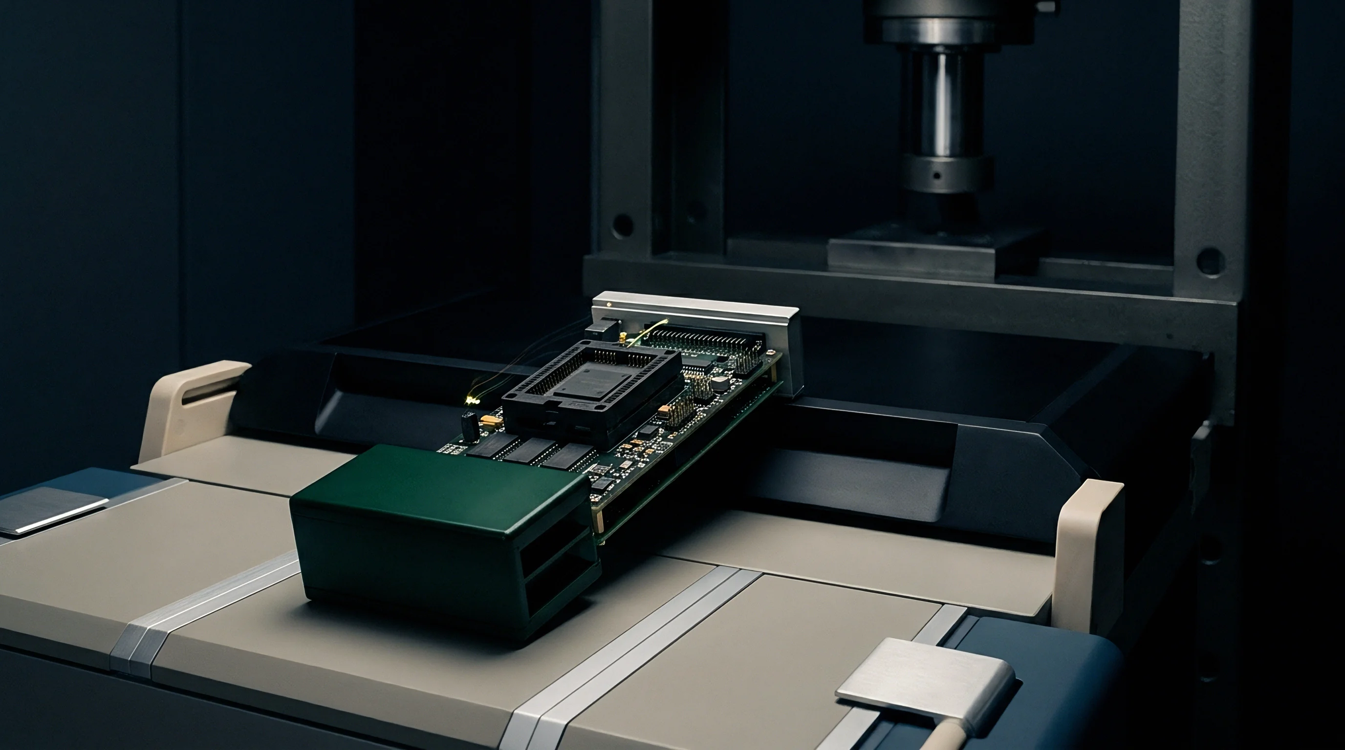
Characterizing RF power stage behavior under dynamic load conditions mandates automated measurement setups capable of sweeping load phase at constant standing wave ratios. Traditional static 50-ohm bench measurements fail to capture the transient waveform distortions that occur during physical radio operation. Modern vector load pull test stations utilize automated electromechanical or active electronic tuners to synthesize precise reflection coefficients at the device reference plane.

Time-Domain Envelope Measurements on Mismatched Drains
Calibrated active load pull systems use wideband vector signal generators paired with high-speed digitizers to capture instantaneous voltage and current waveforms. By injecting controlled reflection signals back into the power amplifier output node, active load pull instruments synthesize arbitrary complex impedances across 360 degrees of phase without mechanical tuner movement latency. Time-domain RF envelope measurements capture the exact instant waveform clipping and phase distortion occur within a modulated burst.
Measurement metrics prioritize Error Vector Magnitude and Adjacent Channel Leakage Ratio under real-world modulation schemes such as Quadrature Amplitude Modulation and Orthogonal Frequency Division Multiplexing. As load phase rotates around a 3:1 standing wave ratio circle, Adjacent Channel Leakage Ratio degrades non-linearly. Phase angles that induce heavy knee clipping generate high spectral sidebands that spill directly into adjacent licensed spectrum channels.
Failure to meet the -30 dBc adjacent channel power ratio specified in ETSI EN 300 328 under mismatched antenna loads invalidates European CE compliance filings.

Procedure for Mapping Phase-Dependent EVM Boundaries
Engineers assessing RF transmitter linearity set up automated sweeps using vector network analyzers linked to programmable load impedance tuners.
- Calibrate the vector network analyzer and load tuner at the primary antenna feed reference plane using standard open, short, load calibration standards.
- Synthesize a constant VSWR circle of 3.1 to 1 across the target operating frequency band in 15-degree phase steps.
- Apply the maximum specified modulated RF input signal to the power stage while capturing peak current draw and thermal baseline temperatures.
- Measure Adjacent Channel Leakage Ratio and Error Vector Magnitude at each discrete load phase coordinate using a digital signal analyzer.
- Record the boundary phase angles where modulation error exceeds protocol standards or thermal current triggers over-temperature shutdown.
| Protocol Band | Standard EVM Limit (%) | Measured EVM Range (%) | Standard ACLR Limit (dBc) | Measured ACLR Range (dBc) | Max PAE Drop (%) |
|---|---|---|---|---|---|
| BLE 5.2 (2.4 GHz) | 20.0 | 4.2 to 24.8 | -20.0 | -15.2 to -32.1 | 18.5 |
| Wi-Fi 6 (2.4 GHz, 20 MHz) | 3.5 | 1.8 to 8.9 | -30.0 | -21.4 to -38.5 | 24.0 |
| LTE-M Band 20 (868 MHz) | 8.0 | 2.1 to 14.2 | -37.0 | -28.1 to -42.0 | 21.2 |
| LoRaWAN (915 MHz) | 10.0 | 3.1 to 16.5 | -28.0 | -22.0 to -34.8 | 16.8 |
| Wi-Fi 6E (5.8 GHz, 80 MHz) | 2.5 | 1.9 to 11.4 | -32.0 | -18.9 to -36.2 | 29.5 |
| Data measured using an automated active load tuner at 25°C ambient temperature with nominal supply voltage. | |||||
Field spectrum violations often trace to phase-induced conduction angle breakdown rather than unshielded board layout.


Transit
Operational environments introduce continuous, highly variable load impedance shifts as miniaturized radios move through physical space. Handheld asset trackers, wearable biometric sensors, and compact cellular modules experience dramatic near-field interaction with surrounding objects. The human body acts as a lossy dielectric material with high relative permittivity, absorbing radiated RF energy and altering the reactive boundaries of tiny internal antennas.

Dielectric Proximity and Real-Time Impedance Drift
Human hands, metal surfaces, and moisture layers placed near small internal antennas alter the localized electric field distribution. Near-field loading shifts the antenna resonant frequency away from the operational carrier frequency, driving the input reflection coefficient away from the center of the Smith chart. As a user changes hand positions or places a radio device against a metallic structure, the load reflection coefficient traces rapid phase orbits at VSWR levels frequently exceeding 5:1.
Battery voltage discharge profiles compound the operational risk of phase-induced conduction shifts. As internal battery cell resistance rises during discharge, high peak current pulses demanded by capacitive load phases cause instantaneous supply voltage droop. Supply droop degrades power amplifier headroom, accelerating knee line saturation and precipitating sudden frame error rate spikes during packet transmission bursts.
- Quantify Maximum Field VSWR Boundaries across expected user hand and body placement configurations using phantom body models before finalizing mechanical housings.
- Verify Tuner Settling Latency against protocol preamble duration to prevent packet header corruption during active impedance adjustment cycles.
- Evaluate Battery Peak Current Limits under low-impedance load phase conditions to avoid triggering internal protection circuits or brownout resets.
- Assess Harmonics Radiation Profiles at extreme reactive phase angles to ensure harmonic filter attenuation accounts for load-induced harmonic generation.

Adaptive Tuning Networks and Phase Compensation Limits
Dynamic Antenna Tuning systems utilizing high-voltage RF-MEMS capacitors or aperture switches rebalance matching networks in real time. Closed-loop tuning systems incorporate directional couplers and phase detectors to measure the complex reflection coefficient at the transmitter output. Processing algorithms evaluate the magnitude and phase of reflected power, instructing variable capacitor banks to synthesize compensating reactive impedances.
Closed-loop adaptation speed limits constrain dynamic tuning performance in fast packet-based radios. Closed-loop tuning networks require between 10 and 100 microseconds to detect phase mismatch, execute control algorithms, and settle variable capacitive elements. Fast modern packet preambles, such as those in Wi-Fi 6 or Bluetooth 5 High Speed modes, transmit critical synchronization data within the first few microseconds of a burst.
If the dynamic tuner fails to settle before preamble transmission completes, receiver synchronization fails, causing immediate packet rejection despite subsequent matching correction.
Enclosure plastic dielectric constant variations shift antenna resonance frequency and rotate the baseline load pull phase vector.
Section 15.247 compliance testing requires radiated spurious emission audits across all antenna operational states, compelling designers to lock dynamic tuners into worst-case phase positions during certification.


Ledger
Procurement specifications and bill of materials calculations must balance RF front-end protection costs against field failure liabilities. Selecting low-cost power amplifier silicon without investigating reactive load phase ruggedness introduces severe commercial risks. While basic power amplifier integrated circuits offer attractive unit prices, their vulnerability to phase-induced conduction angle breakdown requires costly board-level mitigation strategies or yields unacceptably high field return rates.

Commercial Tradeoffs in Ruggedized PA Silicon Sourcing
Selecting power amplifier integrated circuits involves weighing raw chip unit price against integrated protection features. Standard Complementary Metal-Oxide-Semiconductor power amplifiers operating near dielectric breakdown boundaries cost significantly less than ruggedized Gallium Nitride or specialized Silicon-Germanium devices designed to survive 10:1 standing wave ratios across all phase angles.
Alternative front-end protection architectures introduce distinct bill of materials and physical board area trade-offs. Inserting a ferrite circulator between the power amplifier and antenna completely isolates the active silicon from load phase variations by absorbing reflected energy in a 50-ohm termination resistor. Ferrite circulators add between 0.80 and 1.50 USD to the landed bill of materials cost, consume up to 9 square millimeters of board area, and introduce a mandatory 0.6 dB insertion loss penalty that permanently reduces battery operating life.
| Mitigation Architecture | Unit BOM Cost (USD) | Board Area (mm²) | Insertion Loss / Efficiency Penalty | Mismatch Phase Immunity |
|---|---|---|---|---|
| Unprotected CMOS PA | 0.25 to 0.45 | 1.5 to 2.5 | None (Baseline) | Poor (Fails ACLR at VSWR > 2.5:1) |
| Rugged GaN PA Stage | 1.10 to 2.20 | 4.0 to 6.5 | Higher thermal dissipation floor | Excellent (Survives 10:1 all phases) |
| Closed-Loop RF-MEMS DAT | 0.65 to 1.30 | 3.5 to 5.0 | 0.4 to 0.8 dB tuner insertion loss | Good (Corrects phase up to 4:1) |
| Integrated Ferrite Circulator | 0.80 to 1.50 | 6.0 to 9.0 | 0.6 dB fixed forward loss | Complete (Decouples load phase) |

Sourcing Dossier Requirements for Dynamic Mismatch Margins
Engineering documentation submitted to contract manufacturers must state explicit mismatch boundaries rather than generic 50-ohm output ratings. Procurement dossiers that omit complex load phase requirements leave projects vulnerable to silicon batch variations. A power amplifier lot produced with slightly higher transconductance may pass nominal 50-ohm production testing while exhibiting severe thermal instability when subjected to reactive phase angles in the finished radio enclosure.
Verification clauses in module supply contracts specify automated load pull compliance sweeps across 24 phase coordinates at a minimum 3:1 standing wave ratio. Qualifying silicon vendors against strict phase-dependent Error Vector Magnitude and Adjacent Channel Leakage Ratio ceilings prevents unexpected field returns. Establishing clear phase ruggedness criteria in technical procurement dossiers ensures delivered radios maintain regulatory spectral compliance regardless of end-user handling patterns.
Whether upcoming cellular IoT standards will mandate standardized phase-pull testing for handheld terminal certification remains an open debate among regulatory committees.