State-Space Thermal Feedforward Compensation for Monolithic Digitally Controlled RC Oscillators
State-space thermal feedforward predicts substrate heat diffusion to apply sub-microsecond frequency corrections, keeping crystal-less RC oscillators within RF spec.
Flux
A power amplifier drawing ninety milliamperes during a Bluetooth Low Energy transmission burst injects twenty-five milliwatts of concentrated thermal dissipation into three square millimeters of silicon. The localized junction temperature climbs four degrees Celsius within twelve microseconds. At thirty megahertz, an uncompensated monolithic resistor-capacitor tank drifts three hundred parts per million over that thermal transient.
When the frequency shifts beyond fifty parts per million, the demodulator on the remote receiver drops the incoming packet preamble. Transmit power, matching circuit impedance, and thermal impedance determine the exact rate of frequency decay, with active drift corrupting phase modulation and widening the spectral emission mask.
Removing the external quartz resonator eliminates two package pins and shaves four cents from the bill of materials. That architectural choice places the full burden of frequency stability onto the silicon substrate. Monolithic diffusion resistors exhibit a typical temperature coefficient of positive eight hundred parts per million per Kelvin, while integrated metal-oxide-metal capacitors shift by positive thirty parts per million per Kelvin across operational ranges.
Without active compensation, ambient temperature swings from negative forty to positive eighty-five degrees Celsius produce a frequency excursion exceeding seven percent. Closed-loop frequency locked loops stabilized against low-frequency reference signals fail during rapid power-up cycles, as feedback loop bandwidth remains constrained below ten kilohertz to prevent excessive phase noise degradation. Thermal transients induced by internal power amplifier switching operate three orders of magnitude faster than the tracking bandwidth of standard analog phase locked loops.
A twenty-five milliwatt power amplifier step produces a frequency slew rate of twenty-four kilohertz per microsecond at an uncompensated center frequency of thirty-two megahertz.
Thermal diffusion through bulk silicon obeys the heat diffusion equation governed by volumetric heat capacity and thermal conductivity. Energy spreads from active transistor junctions through the metallization layers down to the substrate paddle. The thermal front reaches the frequency-determining passive structures with a transport delay governed by physical separation distance.
That propagation delay destroys the phase margin of classic negative feedback compensation networks, where direct feedback based on remote temperature sensing creates oscillatory corrections around the nominal frequency. Feedforward compensation avoids this by calculating the required tuning word before heat reaches the resonant tank, using a digital engine to model heat propagation through discrete volumetric blocks.
- Thermal settling overshoot occurs when a feedback loop applies correction after the local heat wave has already washed past the capacitive array.
- Varactor modulation distortion arises when local substrate heating alters the depletion capacitance across tuning diodes unevenly.
- Spectral mask leakage happens during rapid thermal slewing as instantaneous frequency shifts spread energy into adjacent wireless channels.
- Packet preamble truncation results from receiver synchronization failure caused by frequency discrepancies exceeding the capture range.
Silicon conducts heat rapidly. The time constant of heat propagation through fifty micrometers of bulk silicon sits near four microseconds. An on-die temperature sensor placed two hundred micrometers away from the oscillator core registers less than ten percent of the thermal step during the initial ten microseconds.
Compensating for that missing thermal energy demands an accurate mathematical representation of thermal propagation across the physical layout. Operating an open-loop lookup table against a delayed sensor reading guarantees frequency error during the transmission burst. When thermal transients drive the instantaneous carrier outside the allocated band edges, regulatory certification testing fails immediately and the lot faces containment.


Matrix
Continuous-time heat transfer within an integrated circuit maps directly into a system of linear differential equations. Discretizing the physical die into lumped thermal nodes yields a classical state-space representation where the state vector represents the temperature of each localized volume. The system matrix models thermal conductance between adjacent silicon blocks and heat dissipation through the leadframe into the circuit board.
The input matrix maps power dissipation from internal heat sources, including the radio frequency power amplifier and baseband digital processing cores. The output equation produces the estimated temperature of the oscillator tank components, which settles within twelve microseconds.
State-space feedforward constructs an internal simulation of the thermal field running synchronously with the digital control clock. The state update equation advances with each cycle of the system clock, calculating temperature distributions across the die in real time. Because the input vector tracks known power states commanded by the link-layer controller, the observer predicts heating before the physical sensor registers a single degree of temperature rise.
The input matrix takes binary transmission flags and instantaneous voltage rail measurements to compute dissipated power. A discrete-time state transition matrix governs the temporal progression of the thermal states across constant sampling periods.
Can State Observers Outrun Thermal Diffusion Delays?
Physical thermal diffusion imposes an absolute time delay proportional to the square of the distance between the heat source and the target node. A classical temperature sensor reports conditions that occurred in the past relative to the heat generation event. The state-space observer overcomes this transport delay by evaluating the dynamic system inputs directly.
When the baseband controller asserts the power amplifier enable line, the input vector reflects that power injection instantaneously, allowing the digital state engine to project future temperature trajectories across the intermediate substrate nodes and update the filter matrix.
A reduced-order model captures dominant thermal dynamics without overwhelming the digital gate count. A third-order state-space model isolates three key physical zones: the power amplifier power stage, the intermediate substrate channel, and the digitally controlled oscillator tank. The discrete formulation evaluates according to standard matrix algebra:
x(k+1) = A_d x(k) + B_d u(k)
y(k) = C_d x(k) + D_d u(k)
Here, x represents the three-element state vector of node temperatures, u represents the input vector of electrical power dissipations, and y represents the estimated temperature at the oscillator core. The matrices A_d, B_d, C_d, and D_d derive from the continuous physical geometry through zero-order hold discretization at a sampling rate of two megahertz.
A feedforward observer predicts thermal shifts by computing substrate power dissipation cycles before temperature sensors respond.
The table below summarizes the thermal time constants and discrete coefficients for a typical third-order silicon realization evaluated across two hundred micrometers of lateral substrate separation under five volts operating potential.
| Model State Node | Effective Time Constant (µs) | Thermal Resistance (°C/W) | Thermal Capacitance (nJ/°C) | Discrete Pole Location (z) |
|---|---|---|---|---|
| Power Amplifier Junction | 1.8 | 42.5 | 42.3 | 0.758 |
| Substrate Boundary | 6.4 | 78.1 | 81.9 | 0.925 |
| Oscillator Tank Core | 18.2 | 115.6 | 157.4 | 0.973 |
Computing the state updates requires integer arithmetic implemented within dedicated hardware registers. Floating-point units consume excessive active area and battery power. Fixed-point representation using eighteen bits of resolution maintains state calculation errors below zero point zero five degrees Celsius.
Truncation noise within the state-space matrix arithmetic translates directly into frequency jitter, so roundoff errors must stay below the least significant bit weighting of the oscillator tuning bank. Computational steps unfold across a disciplined sequential order:
- The baseband controller writes instantaneous power dissipation values into input registers across the peripheral bus.
- The arithmetic logic unit multiplies the input vector against the discretized input matrix using sixteen-bit coefficients.
- Previous state registers update through accumulation with the state transition matrix product.
- The observer projects the output temperature vector toward the oscillator compensation decoder logic.
Unmodeled physical variations compromise state-space accuracy over wide manufacturing lot distributions. Packaging bond wire thickness, mold compound thermal conductivity, and solder voiding under the thermal pad shift the discrete poles away from their nominal mathematical coordinates. Whether an on-chip continuous calibration engine can update the state transition matrix during long deployment lifecycles without disrupting live radio links remains unresolved.

Die
Silicon layout choices dictate the magnitude and phase of thermal coupling between sub-circuits. Placing the frequency-generating tank adjacent to the radio frequency output stage maximizes the thermal step and shortens diffusion time. Placing the tank at the opposite end of the silicon floorplan increases propagation delay and introduces attenuation into the thermal impulse.
Thermal layout symmetry minimizes uneven temperature distribution across balanced passive components, while interdigitated finger layouts for metal-oxide-metal capacitors equalize the thermal gradient across differential nodes.
Substrate trench isolation alters heat flow lines through the bulk material. Deep trench isolation rings etched into silicon create partial barriers to lateral heat flux, directing energy downward into the heavily doped substrate bulk. Packaging architecture alters the boundary conditions of the heat equation.
A quad flat no-lead package with an exposed center pad provides a low-impedance thermal exit into the copper ground plane of the printed circuit board. A chip-scale package forces heat to leave through minute solder balls, elevating thermal resistance by forty degrees Celsius per watt. In heavily potted assemblies, such as those found in industrial sensor nodes or automotive engine controls, heat accumulates rapidly because external potting resins exhibit thermal conductivities three orders of magnitude lower than copper ground planes.
Thermal pad solder coverage below seventy percent doubles transient temperature rise during sustained transmission bursts.
The physical temperature sensor requires strategic placement relative to the heat source and the oscillator tank. Placing the sensor directly inside the power amplifier cell measures source dissipation but misses substrate transfer dynamics. Placing the sensor inside the oscillator core introduces parasitic capacitance and degrades the loaded quality factor of the resonant tank.
Split-sensor architectures place one sensing diode near the heat source and a secondary diode inside the oscillator periphery, allowing the state-space engine to process the delta between both sensors and calibrate ambient offsets against dynamic switching surges.
| Package Configuration | Thermal Resistance Junction-to-Case (°C/W) | Observed Latency Delay (µs) | Max Observer Slew Error (°C) | Residual Drift (ppm) |
|---|---|---|---|---|
| QFN-32 Exposed Pad | 28.4 | 3.8 | 0.35 | 14.2 |
| WLCSP-25 Ball Grid | 68.2 | 8.6 | 1.12 | 46.8 |
| SOIC-16 Leadframe | 95.0 | 14.2 | 2.45 | 102.5 |
Factory calibration procedures capture the static temperature coefficients of the integrated oscillator components. Automated test equipment sweeps the ambient chuck temperature from negative twenty to positive seventy degrees Celsius, recording frequency tuning words at five-degree increments. That procedure fits a third-order polynomial to the static frequency-temperature curve while ignoring dynamic thermal gradients completely.
Dynamic tracking capability depends on matching the state-space matrix parameters to the physical transfer function of the packaged silicon assembly.

Ladder
Frequency synthesis in a digitally controlled oscillator relies on segmented banks of switchable passive components. Switched capacitor arrays implement discrete frequency stepping by connecting tiny metal plates to ground through low-resistance field-effect transistors. The total capacitance divided into binary-weighted and thermometer-coded segments determines tuning range and frequency resolution.
Resistor arrays in relaxation oscillators modulate charging currents directed into integrating capacitances, though channel on-resistance shifts with junction temperature as switch resistance drops, introducing an unwanted thermal coefficient directly into the tuning structure.
Coarse tuning segments cover gross manufacturing process spreads that shift baseline frequency by plus or minus twenty percent across foundry process corners. Fine tuning segments compensate for ambient environmental temperature swings, while an ultra-fine fractional tuning stage eliminates discrete frequency steps that generate phase discontinuities. A delta-sigma modulator clocked at sixty-four megahertz dithers the least significant capacitor unit, yielding an effective resolution of zero point one parts per million.
Quantization noise from the delta-sigma dithering engine must fall outside the receiver channel filter bandwidth to prevent receiver desensitization.
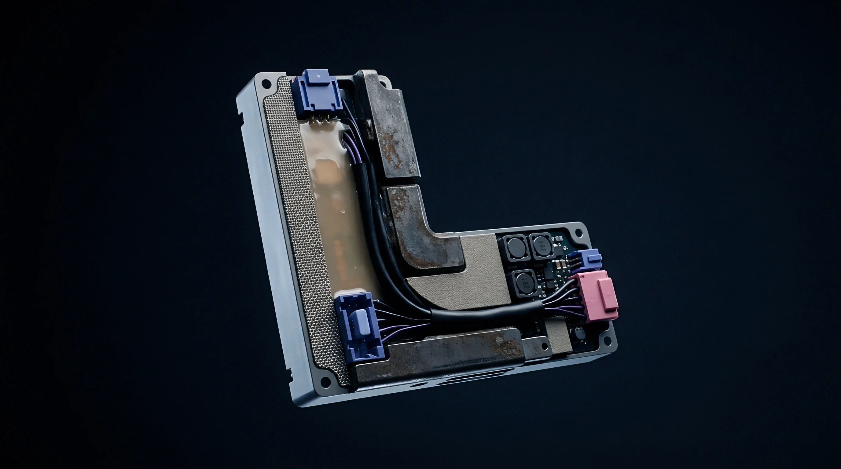
Will Fractional Dithering Induce Spurious Sidebands?
High-frequency dithering of switched capacitive elements modulates the tank impedance cyclically. That modulation folds high-frequency digital switching noise into the oscillation frequency spectrum, creating discrete fractional spurs. When the dither rate correlates with data modulation rates, the spurs degrade adjacent channel selectivity in receiver modes.
Applying a third-order MASH delta-sigma architecture shapes quantization noise toward higher offset frequencies where the passive filtering of the tank provides native attenuation. Fractional dithering keeps the effective step size small while avoiding physical sub-femtofarad capacitor structures that foundry processes cannot reproduce reliably.
The state-space observer produces an eighteen-bit temperature estimation word at every execution step. The compensation decoder maps this estimated temperature onto a sixteen-bit digital control word via polynomial coefficients stored in non-volatile memory. The mapping function addresses linear, quadratic, and cubic temperature dependencies:
DCO_WORD(T) = C_0 + C_1 (T – T_0) + C_2 (T – T_0)^2 + C_3 (T – T_0)^3
The digital control word routes directly to the thermometer decoders and the delta-sigma fractional engine without passing through intermediate registers that introduce clock latency. Feedforward delay from observer calculation to capacitor switch actuation must remain below fifty nanoseconds to preserve transient tracking accuracy. A well-designed switched array maintains uniform capacitor sizing throughout the thermometer section.
Tuning bank design demands strict procedural balance across competing silicon constraints:
- Capacitor segment matching limits raw differential nonlinearity below zero point five least significant bits.
- Switch transistor scaling minimizes series resistance while restricting parasitic drain capacitance to ground.
- Substrate tap density prevents digital transient ground bounce from modulating the internal oscillator core supply.
Calibrated steps determine the ultimate stability of the carrier. When the smallest discrete capacitance step exceeds the maximum allowable frequency deviation, the oscillator output jumps between discrete states continuously. That hunting behavior introduces high-frequency phase jitter that degrades receiver error vector magnitude.
Fine capacitor units must measure smaller than three hundred attofarads.

Budget
Operating a monolithic wireless node without an external quartz crystal alters both the power consumption profile and the RF link margin. A thirty-two kilohertz quartz crystal oscillator draws approximately one microampere continuously during sleep states. An on-chip RC sleep timer draws fewer than one hundred nanoamperes, slashing sleep current by ninety percent.
The RC oscillator drifts by thousands of parts per million across ambient temperature sweeps, forcing the receiver to widen its listening window during scheduled wake-up intervals. Widening the reception window forces the receiver to stay active for longer durations, consuming battery energy to search for incoming preambles.
In Bluetooth Low Energy peripheral connections, the anchor point specifies the exact time a peripheral must wake to receive packets from a central device. The sleep clock accuracy determines the required window widening. Standard quartz oscillators guarantee plus or minus fifty parts per million accuracy, requiring an active window extension of a few hundred microseconds after a one-second sleep interval.
An uncompensated RC oscillator exhibiting five hundred parts per million drift demands a window widening of one millisecond, during which the radio burns thirty milliwatts of power listening to empty air.
State-space thermal feedforward reduces dynamic drift during the active phase while a calibrated low-frequency observer stabilizes the sleep state. During active radio bursts, maintaining frequency within twenty parts per million prevents packet loss and eliminates costly packet retransmissions. Retransmissions cost airtime and drain limited cell capacity.
Carrier stability directly dictates packet error rates across standard wireless communication standards.
A receiver forced to widen its listen window to compensate for sleep clock drift consumes more average power than an active crystal oscillator saves.
The operational balance shifts across radio communication standards, as detailed in the performance matrix below. Calculations assume an ambient temperature transient of twenty degrees Celsius induced by a sustained ten-decibel-milliwatt power amplifier transmission.
| Radio Standard and Modulation | Carrier Tolerance Limit (ppm) | Max Allowable Slew (kHz/ms) | Uncompensated Packet Error Rate (%) | State-Space Compensated PER (%) |
|---|---|---|---|---|
| Bluetooth Low Energy 2M PHY | ±50 | 15.0 | 68.4 | 0.8 |
| IEEE 802.15.4 O-QPSK 2.4 GHz | ±40 | 10.0 | 84.2 | 1.2 |
| LoRaWAN SF12 125 kHz BW | ±25 | 1.5 | 96.5 | 2.1 |
| Proprietary Sub-GHz FSK 50 kbps | ±30 | 5.0 | 72.0 | 1.0 |
In LoRa chirp spread spectrum modulation, an uncompensated thermal frequency slew during packet transmission translates directly into symbol timing errors. Because the chirp rate represents data symbols through instantaneous frequency sweeps, an underlying thermal slope alters the detected chirp slope. That distortion causes the demodulator to miscalculate symbol indices, triggering cyclic redundancy check failures at the gateway.
Feedforward state compensation flattens the frequency trajectory across the entire seventy-millisecond transmission packet.
A supplier providing crystal-less radio frequency modules must demonstrate compliance with regional spectral emission regulations under maximum output power conditions. Sourcing specifications mandate that delivered radio frequency transceivers satisfy ETSI EN 300 328 Section 4.3.2.9 for transmitter frequency range stability under internal thermal transient loads before acceptance testing clears the batch for production assembly.