Sub-GHz Transceiver Pierce Oscillator Gain Margin Optimization under Low-Power Drive
Maintaining a Pierce oscillator gain margin above five under minimum transconductance bias prevents cold-temperature startup failures in sub-GHz IoT transceivers.

Quartz
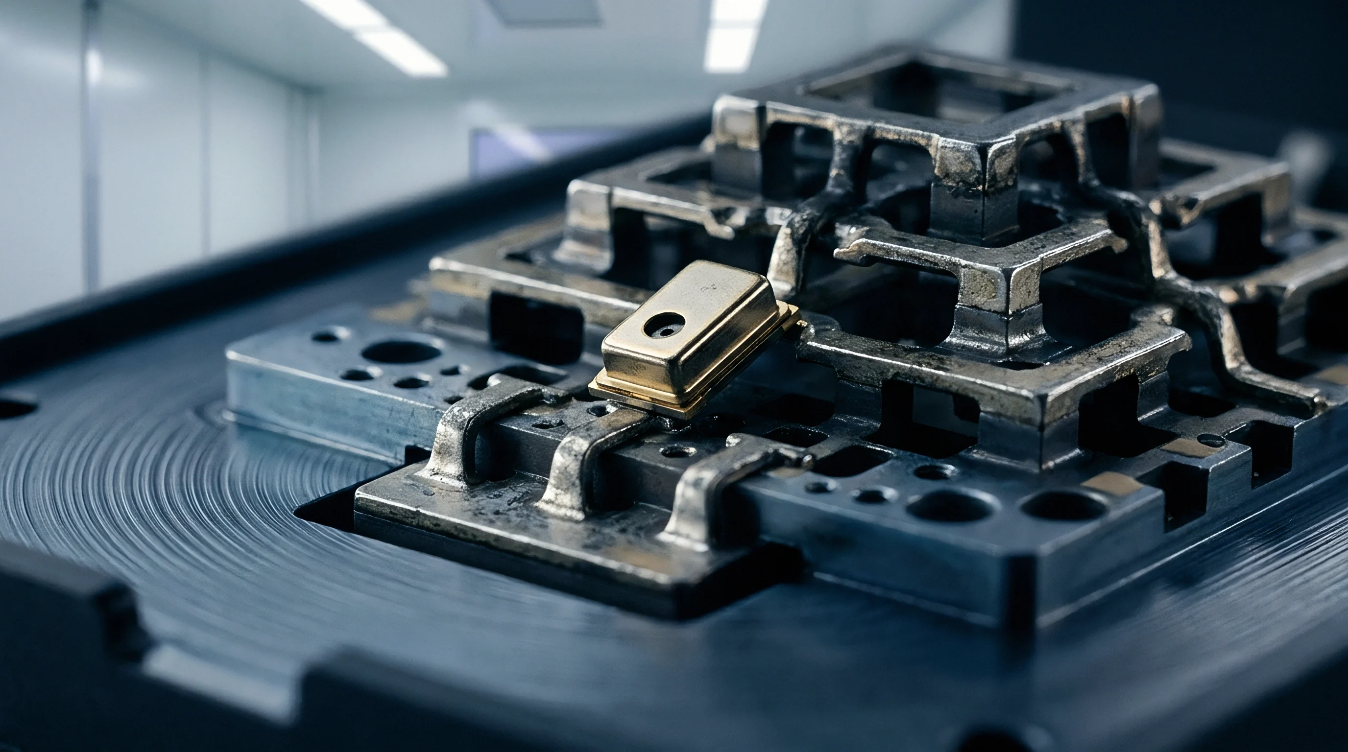
Piezoelectric crystal units in sub-gigahertz radio applications establish the reference frequency for synthesized local oscillators. In low-power transceivers operating in the 433 MHz, 868 MHz, and 915 MHz bands, the primary reference crystal typically operates at fundamental frequencies between 26 MHz and 32 MHz. Achieving long battery life requires minimizing active current in the internal Pierce oscillator amplifier.
Reducing amplifier current lowers transconductance, directly compressing the available loop gain margin needed to guarantee oscillation under worst-case industrial conditions.
Resonator Mechanics under Sub-Milliwatt Bias
Miniature surface-mount crystal units operated at 26 MHz or 32 MHz exhibit electrical parameters that govern oscillator stability. The equivalent electrical circuit consists of motional inductance, motional capacitance, equivalent series resistance, and parallel shunt capacitance across the package terminals. As package footprints shrink from 3225 down to 2016 and 1612 sizes, physical crystal blank areas decrease.
This dimension reduction raises equivalent series resistance from historical baselines of 15 ohms up to 60 or 100 ohms in ultra-small packages.
At low ambient temperatures, equivalent series resistance rises significantly while amplifier transconductance decreases due to temperature-dependent mobility changes in silicon. When evaluating low-power transceivers, total crystal drive power must remain within manufacturer limits to prevent long-term frequency drift and mechanical stress damage.
At minus forty degrees Celsius, small surface-mount crystal packages demonstrate equivalent series resistance increases up to forty percent above room temperature baseline values.
To prevent overdriving while maintaining steady oscillation, circuit parameters must remain within strict bounds across all operating conditions.
- Equivalent series resistance increases sharply as physical package dimensions drop below two millimeters.
- Shunt capacitance creates an alternate current path that diverts gain away from the motional branch.
- Motional capacitance governs energy storage rates within the crystal lattice during transient startup.
- Drive level limits bound the maximum power dissipation to protect crystal blanks from permanent mechanical alteration.
Operating a crystal unit beyond its rated drive power accelerates mechanical aging and induces frequency shifts that breach regulatory channel bandwidth masks.

Transconductance
Active amplifier stages inside low-power sub-gigahertz transceivers supply the energy needed to overcome loop losses in the feedback path. The internal amplifier operating in a Pierce configuration acts as a voltage-controlled current source characterized by its transconductance parameter. Low-power transceiver architectures limit steady-state amplifier current to values between 100 microamperes and 1 milliampere to protect the overall power budget, which directly constrains transconductance magnitude.
Gain Margin Verification and Resistance Ratios
Oscillation capability is quantified by evaluating the ratio between real negative input impedance and crystal series loss. The negative resistance generated by the active Pierce circuit depends on amplifier transconductance, operating frequency, and total load capacitance. The simplified negative resistance calculation models loop gain behavior:
R_neg = – g_m / (2 pi f (C_0 + C_L))^2
In this relationship, g_m represents amplifier transconductance in amperes per volt, f is the operating frequency in hertz, C_0 represents crystal shunt capacitance in farads, and C_L represents the total effective load capacitance presented to the crystal terminals. Oscillation occurs when the magnitude of real negative resistance exceeds the equivalent series resistance. Standard practice establishes a gain margin ratio, defined as K_m = |R_neg| / ESR, where a minimum factor of five is required to guarantee reliable oscillation across component variation, aging, and thermal extremes.
Consider a worked calculation for a sub-gigahertz node utilizing a 32 MHz crystal with an equivalent series resistance of 50 ohms, shunt capacitance of 1.2 picofarads, and total load capacitance of 10 picofarads. The combined parallel capacitance C_0 + C_L totals 11.2 picofarads. The critical transconductance threshold required just to initiate oscillation is computed as:
g_m_crit = 4 (pi)^2 (f)^2 ESR (C_0 + C_L)^2
Substituting the circuit parameters yields:
g_m_crit = 4 (3.14159)^2 (32 10^6)^2 50 (11.2 10^-12)^2 = 2.535 10^-4 A/V
This reveals a critical transconductance of 253.5 microamperes per volt. Achieving a target gain margin ratio of five demands an active transceiver transconductance of 1.268 milliamperes per volt. If internal transceiver bias circuits limit steady-state transconductance to 500 microamperes per volt to minimize battery drain, the resulting gain margin drops to 1.97.
A gain margin below two leaves the circuit vulnerable to startup failure when low temperatures elevate crystal resistance.
Designing for high gain margin ensures robust oscillator startup across raw component manufacturing tolerances.
The relationship between transceiver active bias, crystal load parameters, and resulting gain margin appears in the comparative data collected across standard sub-gigahertz operational profiles.
| Transceiver Bias Level | Transconductance (µA/V) | Load Capacitance C_L (pF) | Crystal ESR (Ω) | Negative Resistance |R_neg| (Ω) | Gain Margin K_m Ratio |
|---|---|---|---|---|---|
| High Boost (Startup) | 5000 | 10.0 | 50 | 985 | 19.7 |
| Standard Nominal | 1500 | 10.0 | 50 | 295 | 5.9 |
| Low Power Steady | 800 | 10.0 | 50 | 157 | 3.1 |
| Ultra-Low Bias | 500 | 10.0 | 50 | 98 | 1.9 |
| Ultra-Low Bias (Cold) | 420 | 12.0 | 70 | 58 | 0.8 |
Selecting load capacitors that balance startup speed against power consumption preserves oscillator reliability across operating temperature bounds.
Startup
Transient energy consumption during crystal activation forms a substantial portion of the power budget in battery-operated radios. Sub-gigahertz transceivers used in smart metering and industrial sensor applications rely on aggressive duty cycling, waking periodically to transmit short data packets before returning to deep sleep. When active transmission lasts only a few milliseconds, the time required for the crystal oscillator to stabilize from zero amplitude directly impacts overall battery life.

Which Load Capacitance Tolerance Prevents Cold-Temperature Oscillator Stall in sub-GHz Nodes?
Tight-tolerance C0G ceramic dielectric capacitors rated to plus or minus zero point one picofarads maintain stable loop impedance under extreme cold. Lowering load capacitance reduces overall loop phase delay, accelerating amplitude growth during startup. Reducing load capacitance increases frequency pulling sensitivity and leaves the node susceptible to stray board capacitance.
Modern transceivers implement dynamic transconductance boosting during the activation phase to address this trade-off.
During startup boosting, internal bias circuits supply high current to the amplifier stage for several hundred microseconds, raising transconductance to several milliamperes per volt. Once internal amplitude detectors confirm stable oscillation, control logic scales back amplifier current to low steady-state levels.
Compliance with European Telecommunications Standards Institute rules mandates carrier frequency precision within ten parts per million for narrow channel allocations.
Auditing crystal activation energy overhead in battery-powered wireless endpoints requires a structured bench evaluation sequence.
- Measure baseline sleep current with a micro-current probe before activating the internal reference oscillator.
- Enable transceiver transconductance boost circuitry to supply peak startup current to the crystal tank network.
- Monitor internal amplitude detector output signals on an oscilloscope to identify oscillation stabilization timing.
- Transition amplifier bias down to steady-state low-power mode once stable oscillation amplitude is verified.
- Measure total active charge consumption during the activation sequence to compute startup energy overhead.
Field startup failures frequently stem from unexpected printed circuit board parasitic capacitance rather than internal transconductance limits.
Topology
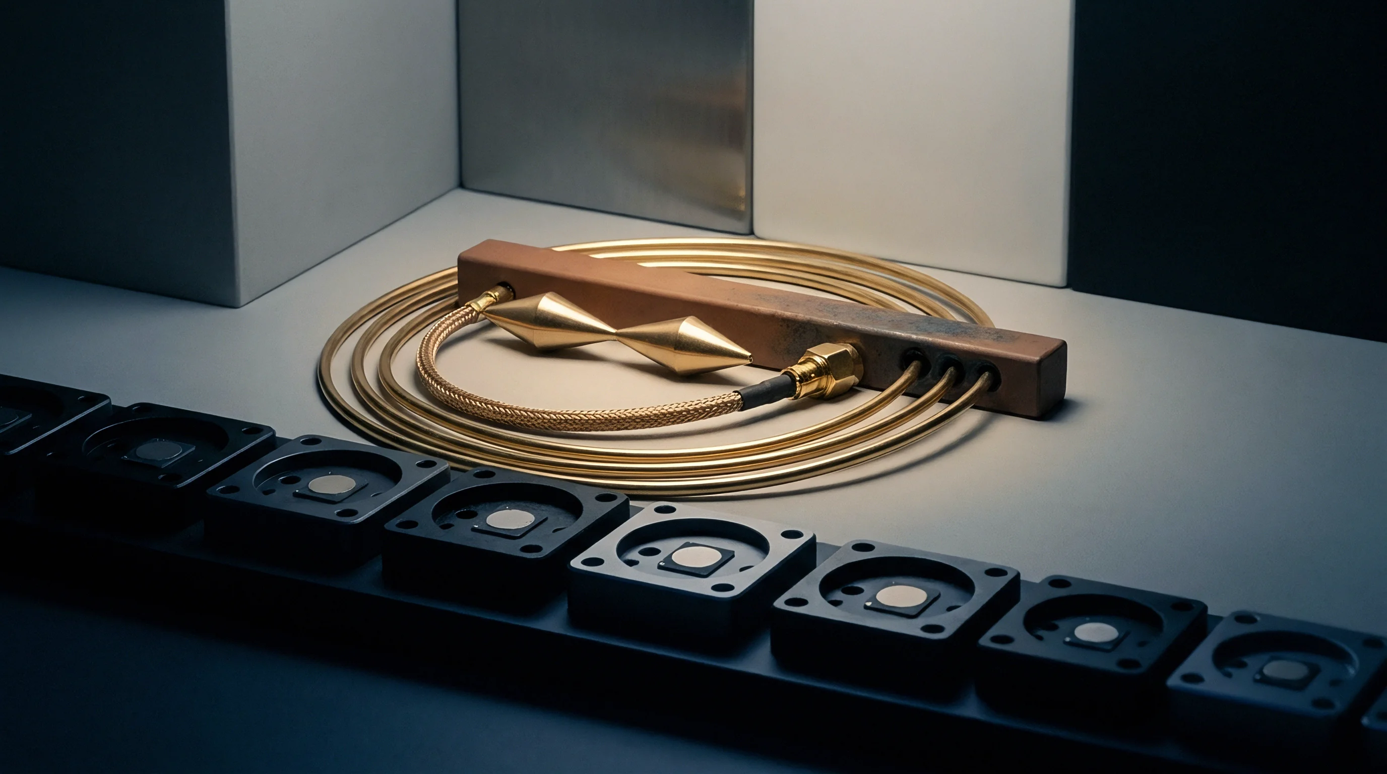
Physical layout choices on printed circuit boards directly influence the total load capacitance seen by the radio oscillator pins. High-frequency parasitic capacitance resulting from long copper traces, internal ground planes, and adjacent component leads alters the effective load capacitance C_L. Unintended additions to load capacitance lower loop gain margin and shift the natural oscillation frequency away from target channel centers.
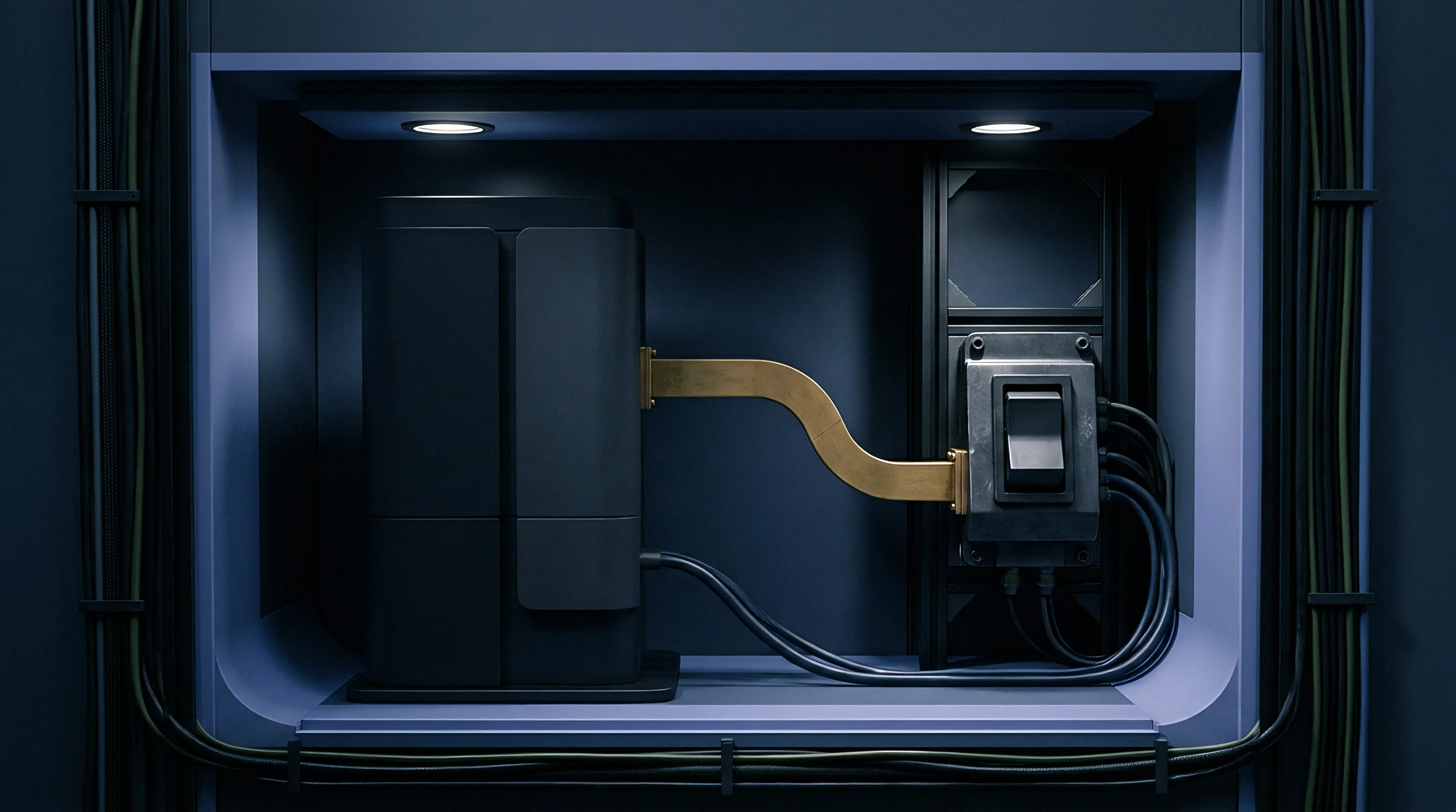
PCB Stray Capacitance and Guard Ring Design
Copper trace geometry between the crystal package and radio terminal pins introduces parasitic capacitance ranging from zero point five to three picofarads. PCB designers place isolated ground guard rings around crystal traces to prevent crosstalk from high-speed digital lines and switching regulators.
Sub-gigahertz standards like LoRaWAN, Sigfox, and Wireless M-Bus enforce narrow spectral masks. Receiver channel filters require tight carrier frequency alignment between transmitter and receiver nodes. Excessive frequency offset degrades sensitivity and increases packet error rates in field deployments.
Trace routing symmetry minimizes differential phase noise and unbalanced capacitive loading across active terminal pins.
The impact of frequency drift and layout-induced loading varies across major sub-gigahertz wireless standards and operational band plans.
| Standard / Protocol | Frequency Band (MHz) | Max Permissible Frequency Offset | Target Channel Spacing | Sensitivity Impact at Max Drift |
|---|---|---|---|---|
| Sigfox Ultra-Narrowband | 868.130 / 902.200 | ±1.5 ppm | 100 Hz | Complete link loss (>10 dB) |
| Wireless M-Bus (Mode N) | 169.400 | ±5.0 ppm | 12.5 kHz | 3.5 dB loss |
| LoRaWAN (BW = 125 kHz) | 868.100 / 915.000 | ±30.0 ppm | 125 kHz | 1.0 dB loss |
| IEEE 802.15.4g SUN FSK | 915.000 | ±20.0 ppm | 200 kHz | 1.8 dB loss |
Board layout considerations for sub-gigahertz radio crystal circuits demand strict adherence to physical routing controls.
- Trace length minimization reduces series inductance and stray capacitive coupling to inner board layers.
- Symmetrical conductor routing ensures balanced loading on both terminal legs of the Pierce oscillator loop.
- Ground plane keepouts beneath crystal pads reduce parasitic shunt capacitance to ground reference layers.
- C0G dielectric selection guarantees thermal capacitance stability across industrial operating ranges.
Section 15.247 of Federal Communications Commission regulations enforces strict fundamental frequency containment that requires precise crystal load capacitance matching across production volumes.

Receipt
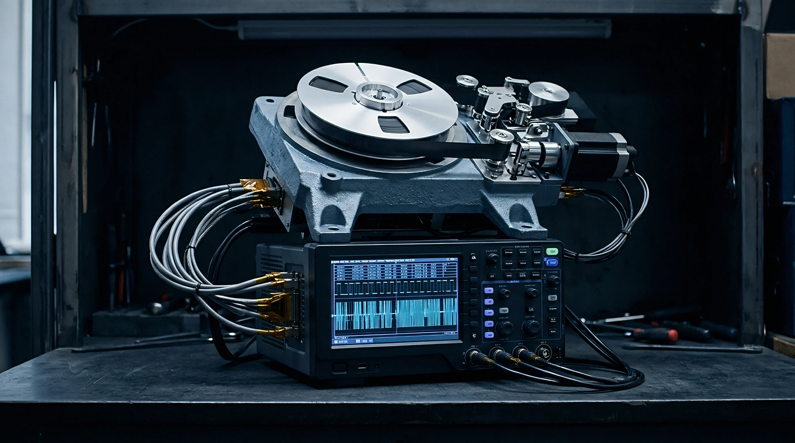
Confirming oscillator stability involves high-impedance active probes and spectrum analysis during environmental stress testing. Direct physical probing of crystal pins with standard oscilloscope probes introduces several picofarads of input capacitance, which pulls the operating frequency and artificially dampens loop oscillation. Accurate measurements require field-effect transistor active probes presenting less than zero point five picofarads of input capacitance or non-contact near-field magnetic probes.

Bench Measurement Techniques and Production Audits
Direct physical measurement of negative resistance involves inserting a variable resistor in series with the crystal unit inside a climate chamber. Testing personnel adjust series resistance during power-up cycles until oscillation fails to start. The sum of the inserted series resistance at stall and the crystal nominal equivalent series resistance defines the total negative resistance magnitude generated by the active transceiver driver.
Production quality processes verify crystal drive margins across silicon wafer fabrication lots and crystal manufacturing batches to maintain high manufacturing yield.
Whether future sub-gigahertz transceivers will integrate fully calibrated internal MEMS resonators to eliminate external crystal drive margin tradeoffs entirely remains an open industrial question.