Meaning
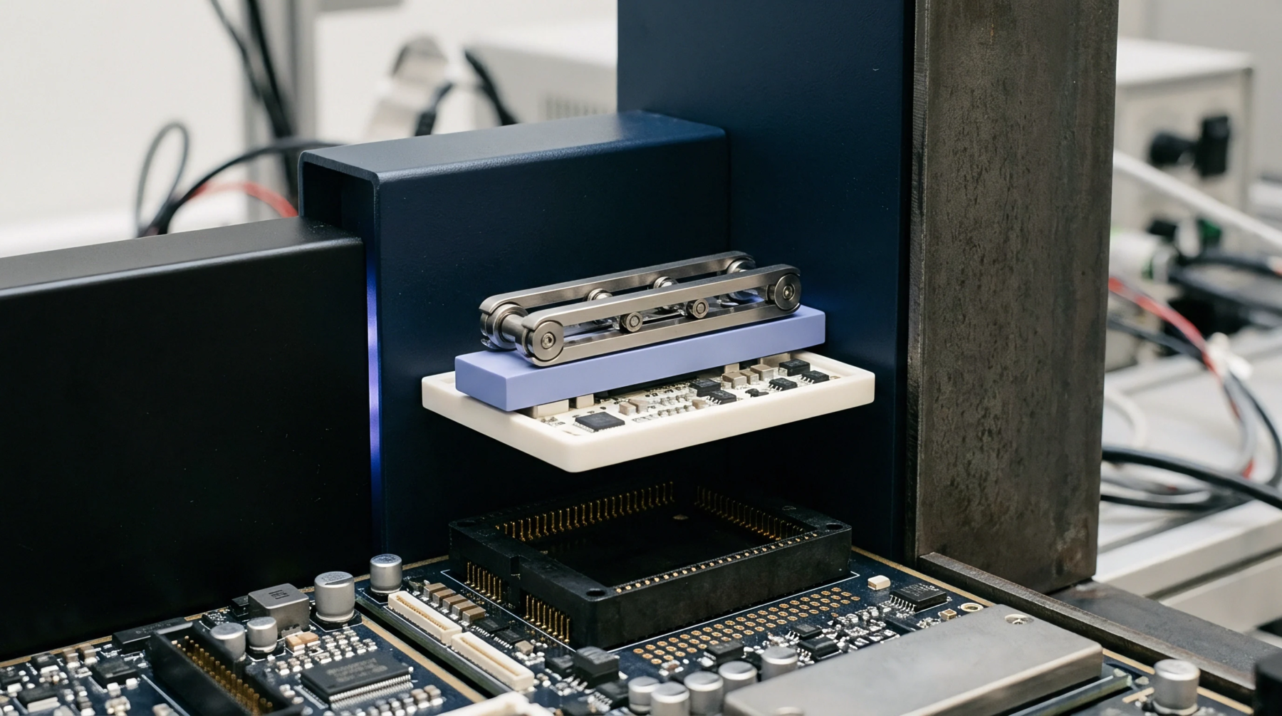
Non-destructive testing of assembled printed circuit boards employs penetrating radiation to image hidden solder joints beneath ball grid arrays and leadless components. High-density automated x-ray inspection systems generate detailed digital images of these concealed connections to evaluate joint integrity on multi-layer boards. This inspection process is applied immediately after the reflow oven to isolate structural assembly errors that are invisible to optical cameras or manual inspection.
Defect Detection
Internal voids, shorts, and solder bridging are identified by analyzing the density of the received radiation. Solder balls that have collapsed improperly under integrated circuits show up as irregular shapes on the digital sensor. These detailed scans allow the manufacturing team to intercept boards that would fail during thermal cycles.
Production Integration
The scanning equipment sits inline between the reflow oven and the final functional test station. Having this diagnostic step integrated directly into the assembly line prevents the accumulation of defective boards in the rework loop. It provides rapid feedback to the screen printing and placement machines to correct drift in solder paste volume.
Solder Assessment
Quality standards define the acceptable percentage of voiding within each individual solder joint. Automated systems calculate this ratio by measuring the grayscale intensity of each joint image. If the void area exceeds the threshold established by IPC specifications, the board is routed automatically to a rework conveyor.