Meaning
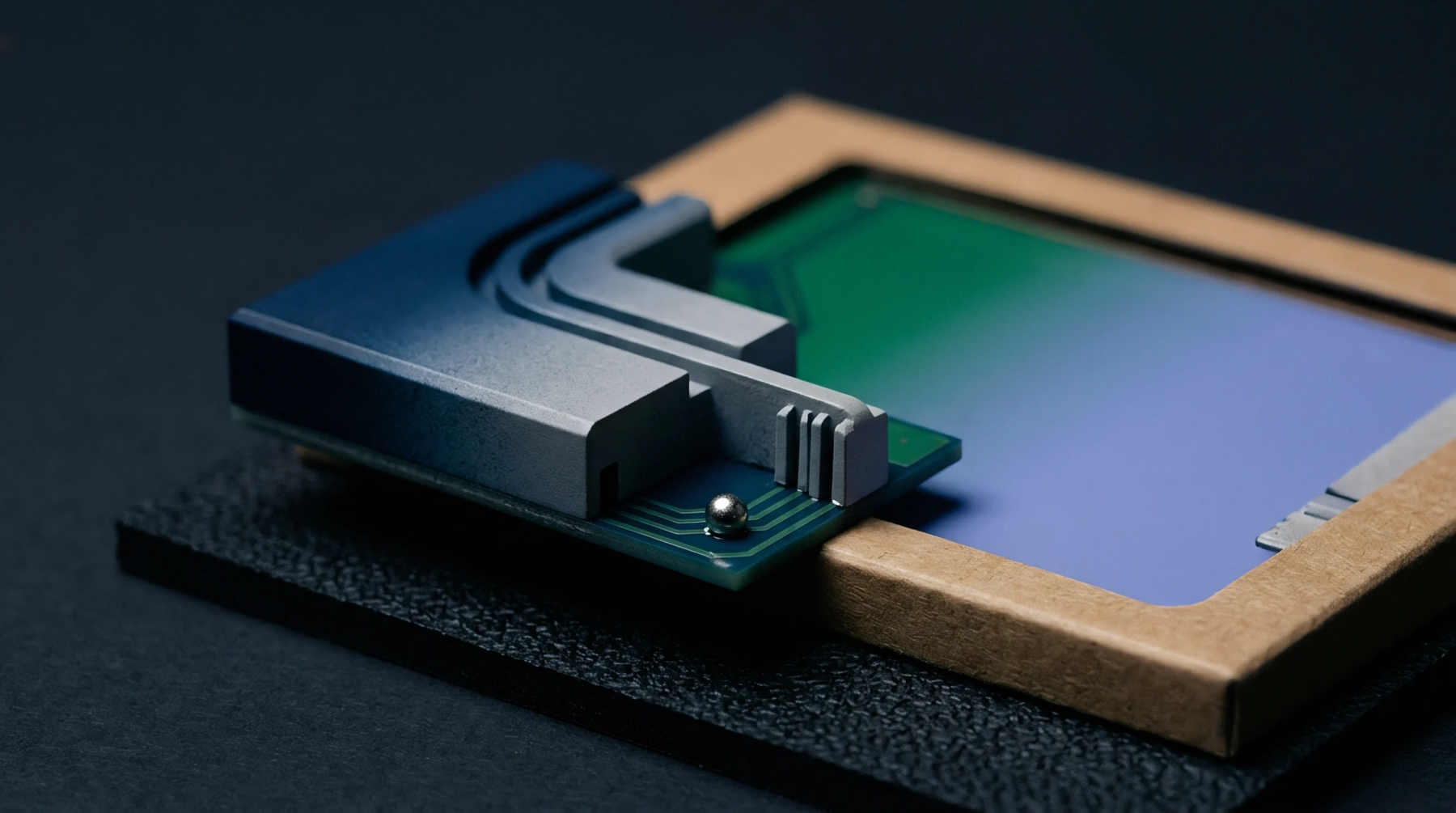
Destructive testing method used to expose the internal structure of a packaged integrated circuit for failure analysis or counterfeiting detection. Decapsulation removes the protective plastic encapsulation or ceramic housing using chemical solvents, lasers, or mechanical abrasion. The process allows technicians to directly inspect the silicon die, bond wires, and lead frame without destroying the electrical path.
Failure Analysis
Physical inspection of the internal die allows engineers to locate cracks, corrosion, or electrical overstress damage. Technicians use this decapsulation process to investigate component failures during reliability testing or field returns. The detailed examination reveals whether the silicon defect originated during die fabrication or during assembly packaging.
Security Evaluation
Verification of authenticity is achieved by comparing the exposed die markings against a known genuine reference sample. Counterfeit chips often show mismatched manufacturer logos or altered part numbers under the microscope after decapsulation has been completed. This physical check represents a decisive step in the qualification of independent-distributor parts.
The process reveals any unauthorized modifications or die-level tampering that would otherwise go unnoticed.
Material Separation
Selective chemical etching requires precise temperature and time controls to avoid dissolving the gold bond wires. Acidic solutions are applied to the package surface until the mold compound dissolves.