Meaning
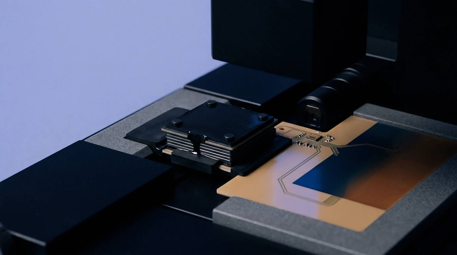
Precision engineered recessed area within a circuit board or semiconductor wafer allows for the embedding of components or the creation of air gaps for acoustic and radio frequency isolation. Creating a micro-machined substrate cavity involves either chemical etching or mechanical milling to achieve specific depths and wall angles. This feature enables a more compact assembly by moving parts from the surface into the body of the carrier.
Designers use these pockets to minimize the overall thickness of the final product while protecting sensitive internal elements.
Dimensional Precision
Tight tolerances on the width and depth of the opening ensure that the inserted component fits securely without excessive adhesive. For sensor applications, the micro-machined substrate cavity provides a protected environment that shields the delicate element from mechanical stress. Measurement systems verify the flatness of the cavity floor to maintain electrical contact integrity.
Thermal Management
Positioning a power hungry chip within a recess brings it closer to internal heat dissipation layers or external cooling surfaces. Mounting a component in a micro-machined substrate cavity reduces the thermal resistance between the silicon junction and the ambient environment. Heat sinks can be mounted directly against the back of the substrate to improve cooling efficiency.
Integration Density
Vertical stacking of components becomes possible when the lower layer is housed within the thickness of the board itself. The micro-machined substrate cavity reduces the total height of the final module, which is necessary for thin consumer electronics. This design allows for shorter interconnects between the embedded chip and the surrounding circuitry.