Establishing Galvanic Isolation Hardware Testing Fixtures for Embedded Drivers
Establishing isolation test fixtures requires slotting substrate barriers, controlling pogo pin parasitics, and enforcing strict NRE source file delivery.
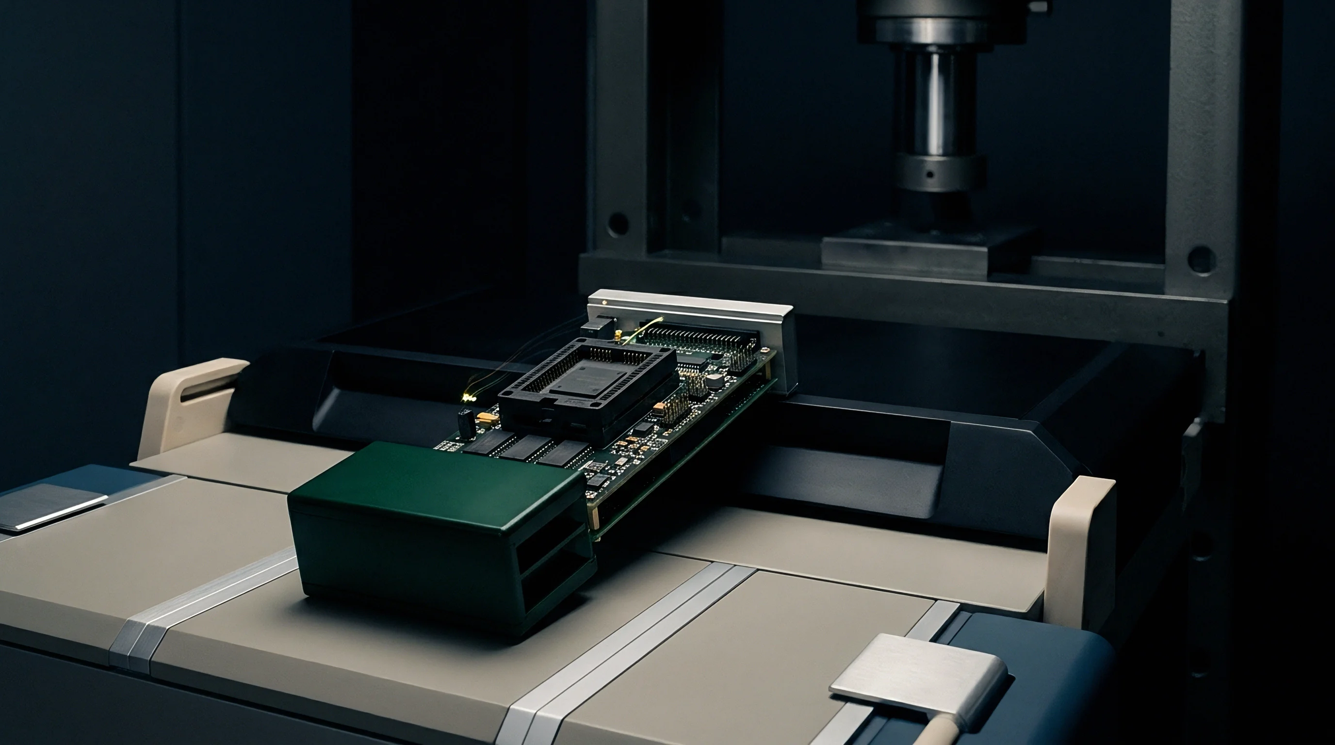

Barrier
Isolation test fixtures need to separate primary control circuits from high-voltage output stages without creating unintended leakage paths across the board. High potential differences across solid dielectrics require enough physical clearance to stop surface tracking and air breakdown during high-voltage surge testing. When evaluating gate drivers rated for 1200V or 1700V silicon carbide switches, compromised clearance from probe placement or socket pin arrays will often break down the fixture before the device under test fails.
Continuous voltage stress across FR-4 or high-Tg polyimide degrades micro-cavities along the glass weave, creating carbonized conductive tracks. Standard design rules for lower-voltage digital boards fall short on galvanic isolation test jigs operating at working voltages above 1000V RMS and transient withstand levels up to 8000V peak.
| Working Voltage (V RMS) | Pollution Degree 2 Creepage (mm) | Clearance in Air (mm) | Minimum FR-4 Cutout Width (mm) | Maximum Allowed Fixture Capacitance (pF) |
|---|---|---|---|---|
| 600 | 6.3 | 5.5 | 3.0 | 1.2 |
| 1000 | 10.0 | 8.0 | 4.5 | 0.8 |
| 1200 | 12.5 | 10.0 | 6.0 | 0.6 |
| 1700 | 17.0 | 14.0 | 8.0 | 0.4 |
Parasitic capacitance across the isolation gap provides a low-impedance path for high-frequency common-mode displacement currents. Running ground planes under the isolation barrier elevates coupling capacitance beyond usable measurement thresholds, masking the driver’s internal capacitance. Similarly, routing trace loops parallel to the isolation slot introduces magnetic coupling that distorts output rise times during rapid pulse tests.
Peak transient withstand testing at 8000V requires a minimum physical air gap of 10 millimeters between primary and secondary copper traces to prevent ionization breakdown across the fixture substrate.
Physical isolation barriers in automated test equipment rely on structural slots routed completely through the fiberglass between high-side and low-side signal domains. Milled air gaps offer higher dielectric strength per millimeter than epoxy substrate materials, though dust and moisture accumulating inside these cutouts reduce insulation resistance over extended testing runs and shift baseline readings.
Dielectric barrier failures in fixtures typically stem from manufacturing residue, poor copper edge plating, or mechanical stress cracks.
- Substrate Delamination Internal layer separation under thermal cycling opens air gaps that ionize well below the bulk dielectric rating.
- Solder Mask Breakdown Liquid photoimageable masks develop pinholes under repeated high-pot testing, shortening effective creepage paths across tight trace spacing.
- Ion Migration High humidity combined with continuous DC bias across the slot drives copper dendrite growth along surface micro-grooves.
- Surface Tracking Carbonization Dust along unsealed slot edges chars from localized partial discharges, forming permanent low-resistance paths.
Uncontrolled creepage and stray capacitance across the board cause false breakdown readings and risk destroying control-side microcontrollers if high-voltage transients bridge the barrier.

Injection
Transient immunity testing subjects the driver to fast voltage ramps applied directly across its galvanic boundary. Common-Mode Transient Immunity evaluations apply high rate-of-change pulses ~ often exceeding 100 to 200 kilovolts per microsecond ~ between primary input ground and secondary power ground. Test fixtures have to deliver these pulses cleanly without overshoot or ringing that could overstress the component.
Board-level pulse generator circuits use ultra-fast gallium nitride FET switches to reach sub-10-nanosecond edge speeds. Any inductance in this layout induces voltage spikes, making it difficult to separate actual driver signal corruption from fixture-generated noise.
| Fixture Sub-Block | Target Parameter | Maximum Permitted Value | Impact of Exceeding Limit |
|---|---|---|---|
| Pulse Generator Loop | Stray Inductance | 4.5 nH | Induces high-voltage edge ringing |
| High-Side Supply Decoupling | ESR at 100 MHz | 15 mΩ | Causes gate driver supply droop |
| Isolated Signal Receiver | Input Capacitance | 2.0 pF | Attenuates fault detection feedback |
| Ground Return Plane | Common-Mode Impedance | 0.5 Ω at 200 MHz | Shifts local signal ground reference |
Differential probing across the isolation gap adds capacitive loading that alters the slew rate of the injected pulse. Dedicated coaxial interfaces mounted directly to the fixture ground plane without long leads preserve signal fidelity during measurements.
Minimizing loop area in the transient injection path prevents high-frequency electromagnetic fields from corrupting low-voltage logic signal monitors during immunity sweeps.
Protecting low-voltage control lines takes multi-layer stackups with inner copper planes acting as Faraday shields around sensitive traces. Running logic lines next to the pulse injection plane allows high displacement currents to couple into control channels. Continuous ground shields divert this displacement current straight back to the pulse generator return without driving current through logic grounds.
Repetitive high-frequency injection causes substantial thermal stress in pulse generator components. Heating alters switch characteristics and degrades edge sharpness during sustained bursts unless active liquid or forced-air cooling keeps fixture temperatures stable, which is necessary for consistent testing across production lots.
Matching the injection loop impedance to the pulse source transmission line prevents standing wave reflections that would otherwise skew measured immunity thresholds.
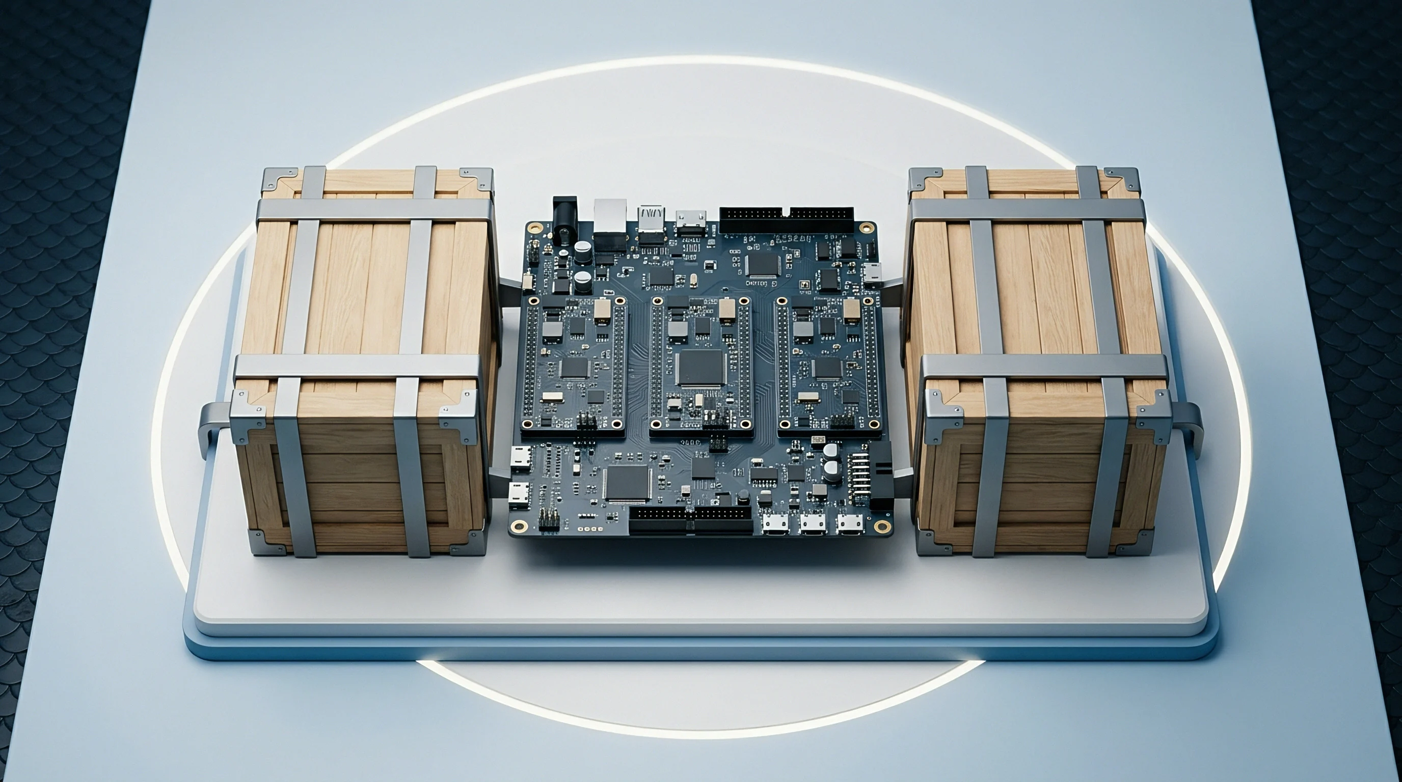
Timing
Gate driver timing determines switching efficiency and protects bridge topologies against destructive shoot-through. Evaluating propagation delay, matching skew, and dead-time control requires fixtures that load output channels with precise inductive and capacitive elements at full operating bus voltage. Parasitics from socket contacts or long traces distort gate current waveforms, masking the actual switching response of the driver IC.
Double-pulse configurations evaluate gate driver response under realistic inductive loads. High-voltage decoupling banks mounted adjacent to the device sockets supply peak gate currents that reach 10 to 15 amperes; any stray trace resistance drops this peak current and skews performance data.
- Connect the coaxial current shunt into the low-side emitter return path using low-inductance surface-mount pads.
- Calibrate high-voltage differential probes against a known 50-ohm pulse source to align propagation skew between voltage and current channels.
- Apply low-voltage logic supply power to the driver primary side while checking quiescent supply current for baseline verification.
- Energize the high-voltage DC bus to the target test voltage with gate drive pulses disabled to measure static leakage.
- Trigger the double-pulse generator to deliver two consecutive logic pulses with microsecond-scale control of pulse width and inter-pulse timing.
- Capture turn-on and turn-off waveforms on a high-bandwidth digital storage oscilloscope to measure propagation delay and rise times.
Inserting coaxial current viewing resistors directly into the power loop minimizes measurement phase lag relative to Rogowski coils or Hall-effect sensors. Placement of these shunts must avoid creating parasitic loops that couple into the gate drive circuit.
Standard IEC 60747-17 mandate 105 section guidelines require absolute propagation delay measurements to account for fixture-induced signal transport delay before certifying isolator performance.
Desaturation detection circuits in isolated gate drivers protect power transistors during short-circuit events. Test fixtures emulate faults using a high-voltage diode network that applies synthetic desaturation voltages to the sense pin during active operation, allowing precise timing of the interval between fault inception and shutdown initiation.
Improperly calibrated timing fixtures obscure internal driver propagation delays, leading to incorrect dead-time programming in end-use inverter controllers.
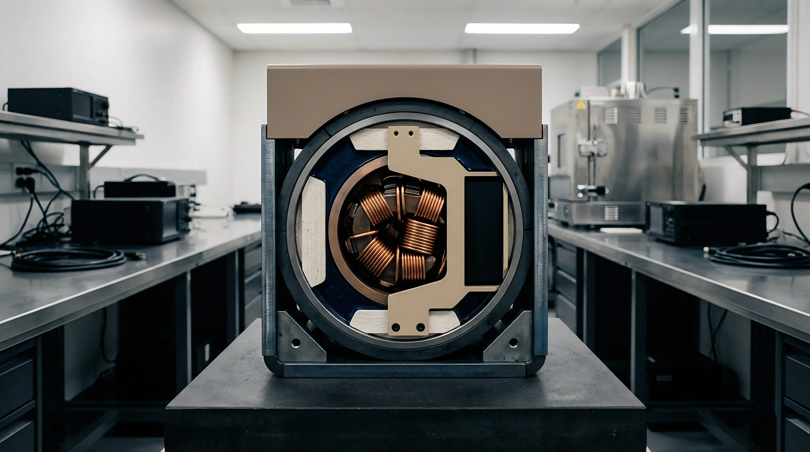
Socket
Production test hardware relies on custom socketing interfaces to cycle ICs through electrical screening without soldering components to the board. Sockets add parasitic inductance, contact resistance variation, and insulation constraints absent in standard surface-mount assemblies. High-voltage isolation testing worsens these issues, since tight pin pitch inside IC sockets concentrates electric fields and accelerates breakdown of the socket housing.
Compression pogo pins accumulate solder fragments and flux residue over thousands of insertion cycles, elevating pin-to-lead resistance from tens of milliohms up to several ohms. This extra resistance drops local driver supply voltage during peak switching transients, triggering false under-voltage lockouts during automated runs.
Self-inductance in pogo pins ~ typically 1.5 to 4.0 nanohenries per pin ~ resonates with driver input capacitance, causing high-frequency ringing on control inputs. Dedicated spring-pin grounding configurations around signal pins dampen this resonance and preserve clean edge transitions on high-speed lines.
Pogo pin contact resistance variation over consecutive insertion cycles alters peak gate drive current delivery, invalidating dynamic switching loss calculations.
High voltage creepage degrades socket pin insulation over extended thermal cycling.
Continuous thermal stress during high-temperature operating life tests degrades the ceramic or PEEK bodies of specialized high-voltage sockets. Micro-cracks between adjacent pin cavities lower the partial discharge inception voltage, triggering micro-arcing during high-voltage screening. Routine partial discharge checks on empty sockets catch insulation wear before fixture defects impact test yields.
Replacing standard sockets with spring-probe assemblies rated for 2500V DC working voltage prevents tracking across narrow lead pitches. Multi-channel isolated drivers with high pin counts impose tight geometric constraints, requiring engineering plastics like Torlon or Vespel to maintain structural rigidity and dielectric strength at elevated temperatures.
Standard dual-in-line test blocks are often rated for 1000V isolation testing, but air ionization across narrow internal pin channels can occur within hours under continuous high-frequency switching conditions.

Scope
Procuring isolation test fixtures requires establishing clear boundaries between internal engineering teams and third-party test integrators. Standard vendor evaluation boards demonstrate driver functionality, but lack the structural shielding, low-inductance probe points, and mechanical durability needed for production validation jigs. Moving from a reference layout to a manufacturing-grade fixture requires explicit deliverable definitions on the contract invoice.
Non-recurring engineering fees for semi-custom test jigs should cover full CAD source files, mechanical fabrication drawings, pulse control board firmware, and calibration records. Accepting a fixture without native Altium or Allegro layout files locks the organization into a single vendor for future board revisions or socket pinhead redesigns.
| Integration Level | Hardware Deliverables | Software and Firmware Scope | Documentation Package | Ownership Boundary |
|---|---|---|---|---|
| Turnkey System | Fully assembled test station, high-voltage pulse generators, socketed DUT mainboard, spare pogo cassettes | Compiled binary executables, automated test sequence scripts, GUI control software | User manual, factory acceptance test report, calibration procedures | Integrator retains schematic IP; buyer receives black-box hardware |
| Semi-Custom Module | Populated mainboard PCB, specialized probe adapters, calibration coupons, mechanical enclosure files | Open-source driver libraries, pulse pattern generator source code, API hooks | Full EDA source schematics, Gerber X2 outputs, fabrication drawings, BOM with vendor parts | Buyer owns board schematics and layout; vendor retains core IP for pulse generator circuits |
| Reference Design Scope | Unpopulated evaluation PCBs, raw gerber files, sample BOM | Example firmware code snippets, basic register setup scripts | Application note, basic schematic PDF | Buyer assumes all engineering liability and manufacturing development risks |
Contractual scope statements must define acceptance protocols for incoming hardware. A complete procedure requires the integrator to demonstrate partial discharge levels below 10 picocoulombs at 1500V RMS, propagation delay repeatability within 200 picoseconds, and pulse generation without ring-back overshoot before final payment is released.
Integrated test systems use dedicated calibration PCBs to verify probe accuracy, baseline fixture capacitance, and DC leakage floors before running IC validation batches. These coupons must accompany the main fixture with factory calibration data traceable to international standards.
The boundary of engineering responsibility ultimately comes down to who resolves parasitic layout discrepancies when test bench measurements diverge from silicon characterization models.
- Gerber X2 Output Packages Complete fabrication files including layer stackup specifications, drill tables, and explicit slot milling paths.
- Native EDA Project Files Full schematics, board layouts, and component databases created in standard CAD formats.
- Mechanical CAD Models STEP files detailing enclosure clearances, socket clamping mechanisms, and safety interlock mounting.
- Firmware Source Repositories Uncompiled C/C++ source code for pulse pattern generators and interlock state machines, along with build environment scripts.
- Validation Test Dossiers Measured baseline calibration curves, partial discharge inception reports, and high-voltage withstand safety certificates.
Determining how far to press integration houses for guaranteed socket lifespan data under combined high-temperature and high-voltage testing helps clarify when internal maintenance liability begins.