Sub Terahertz Passive Intermodulation Measurement in Precision Flange Interfaces
Sub-terahertz passive intermodulation in waveguide flanges is controlled by sub-micron surface finish, precise fastener torque, and tunneling barrier mitigation.
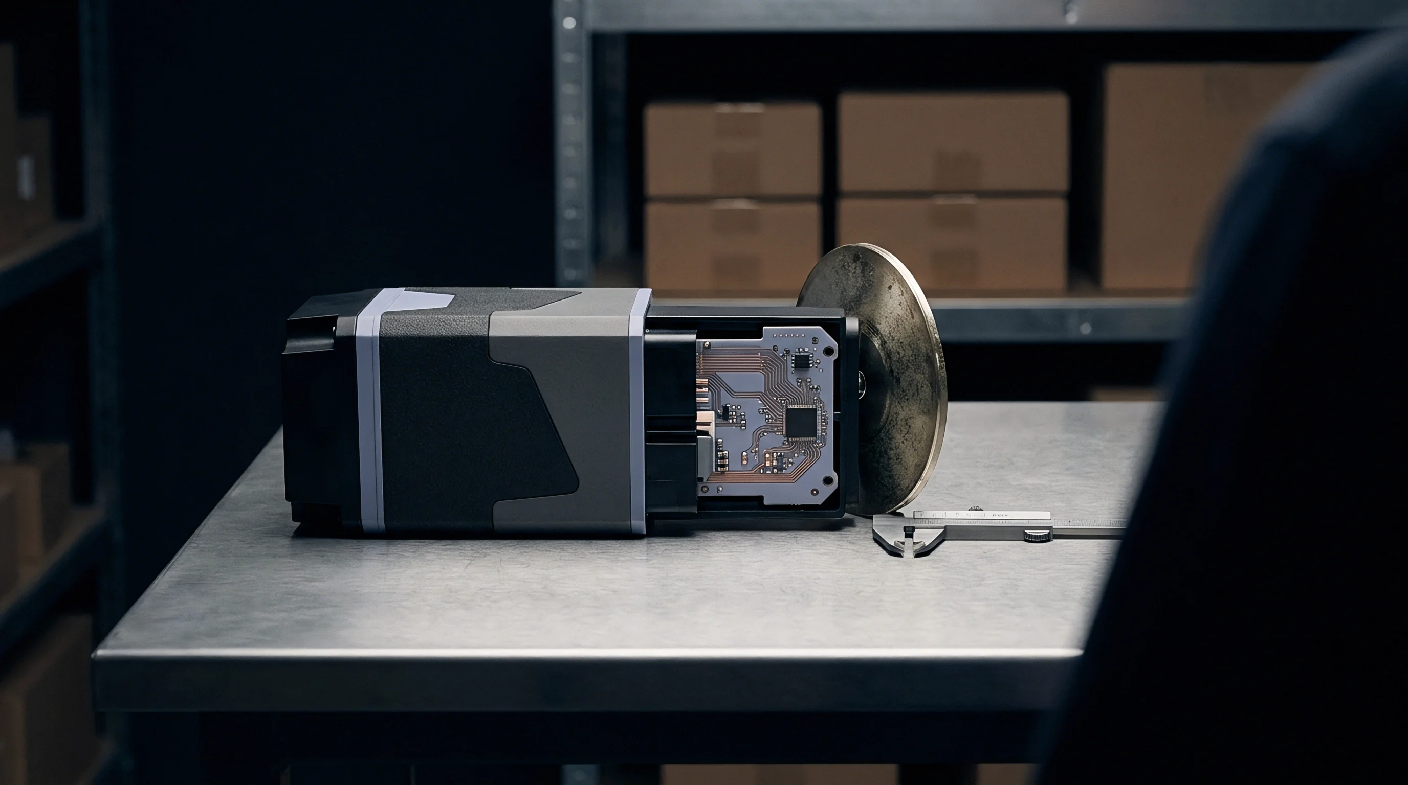

Surface
Sub-terahertz wave propagation through waveguide flange joints depends on physical contact mechanics across microscopic material boundaries. At frequencies from 110 GHz to 330 GHz ~ covering waveguide bands WR-8 through WR-3.4 ~ the electromagnetic field resides entirely within a skin depth thinner than a fraction of a micrometer, so surface topography directly dictates current paths. When two flange faces connect under clamping force, the real contact area is only a minute fraction of the apparent geometrical area.
High-power multi-carrier signals passing through these contact points suffer non-linear mixing, generating passive intermodulation products.

Skin Depth Limits and Micro-Topography Mechanics
Above 100 GHz, currents travel within a metallic layer thinner than 300 nanometers. In high-purity oxygen-free copper, skin depth drops to 0.17 micrometers at 140 GHz and 0.13 micrometers at 220 GHz. Peak-to-valley roughness (Ra and Rz) greater than the localized skin depth disrupts current continuity across the joint, forcing current lines to squeeze through microscopic contact spots ~ asperities ~ and causing sharp spikes in current density.
Even with diamond-turned nanometer finishes, surface roughness that exceeds the skin depth causes non-linear resistance to rise sharply at high power levels. Micro-constrictions at asperity contacts create microscopic voltage drops that scale non-linearly with drive current, generating third-order intermodulation products (2f1 – f2 and 2f2 – f1) directly inside the interface plane.
Surface roughness exceeding skin depth converts linear conductor interfaces into power-dependent non-linear mixing nodes.
| Waveguide Standard | Frequency Range (GHz) | Copper Skin Depth (μm) | Recommended Ra (μm) | Dominant PIM Generation Mechanism |
|---|---|---|---|---|
| WR-8.0 (UG-387/M) | 90 ~ 140 | 0.21 ~ 0.17 | < 0.10 | Asperity constriction resistance non-linearity |
| WR-5.1 (UG-387/M-P) | 140 ~ 220 | 0.17 ~ 0.13 | < 0.05 | Thin-film native oxide electron tunneling |
| WR-3.4 (Precision) | 220 ~ 330 | 0.13 ~ 0.11 | < 0.025 | Micro-gap dielectric breakdown and micro-arcs |
Precision machining leaves microscopic residual stresses and work-hardened layers beneath the flange face. As higher frequencies shrink skin depth further, end-mill marks form parallel micro-grooves that act as periodic non-linear barrier arrays when oriented transverse to RF surface current vectors. Factory visual polish does not guarantee electrical linearity, as worn milling inserts produce microscopic subsurface work hardening.


Junction
Mating two precision metallic waveguide faces creates an uneven interface of localized oxide barriers and direct metallic contact points. RF current crossing this boundary encounters both ohmic paths and capacitive tunneling gaps, where surface oxidation, hydrocarbons, or particulates introduce non-linear voltage-current transfer functions that generate spurious intermodulation tones.
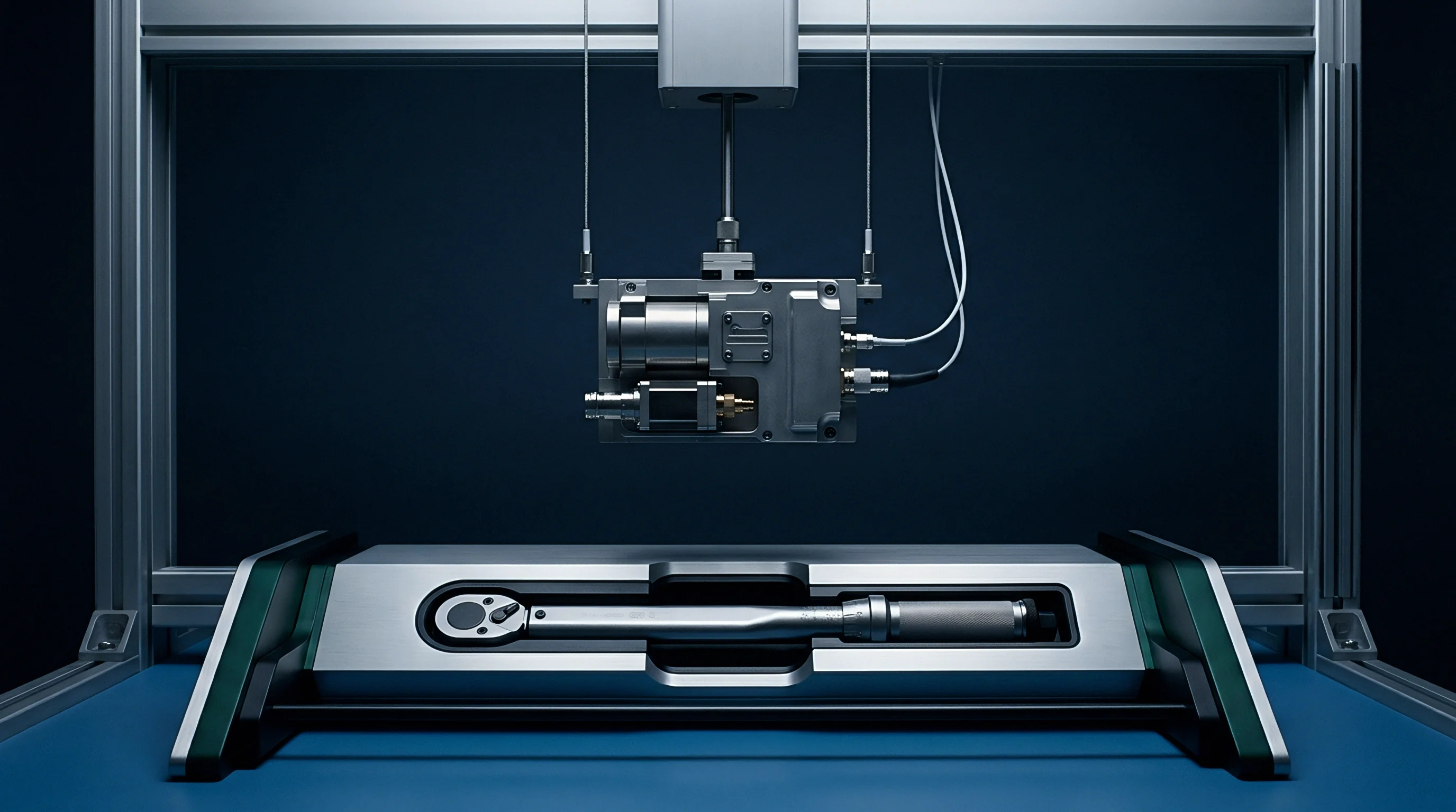
Where Does Micro-Capacitous Tunneling Dominate Junction Intermodulation?
Exposed to ambient atmospheric oxygen, native copper oxides form a thin dielectric barrier between asperities. Cuprous oxide (Cu2O) acts as a semiconductor with a bandgap of approximately 2.1 eV, creating Metal-Insulator-Metal (MIM) diodes across microscopic contact boundaries. When multi-tone RF signals at milliwatt power levels propagate through the flange, field intensity inside 1-to-3-nanometer oxide gaps reaches thousands of volts per millimeter.
The resulting micro-arc discharges and electron tunneling through these ultra-thin oxide barriers create a non-linear current response, producing intermodulation tones that re-radiate into the waveguide transmission channel.
A two-tone input of +15 dBm per carrier at 170 GHz generates -115 dBm third-order intermodulation products across an interface with 1.2 micrometers peak-to-valley roughness.
Interface degradation follows several distinct structural and chemical failure pathways during assembly and operational lifecycle exposure:
- Native Oxide Tunneling thin cuprous oxide films create Metal-Insulator-Metal junction barriers across non-contact gaps, generating odd-order intermodulation products under multi-tone excitation.
- Micro-Swarf Entrapment airborne metallic dust and machining debris trapped between flange faces concentrate mechanical load onto single point discontinuities, accelerating local plastic deformation.
- Asperity Thermal Expansion Shift differential thermal movement across the mating plane shifts localized contact points, causing unpredictable step changes in passive intermodulation amplitude during temperature swings.
- Galvanic Corrosion Couples dissimilar plating materials like gold over nickel flash establish localized galvanic potential differences, accelerating surface degradation in humid operating environments.
Micro-swarf and solder flux residues trigger sudden non-linear breakdowns, while dirt or skin oils deposited during manual handling burn under high RF power, leaving carbonized tracks that act as non-linear resistors. Although tight tolerances reduce interface reflections, the extent to which cryogenic cooling suppresses thin-film oxide tunneling across sub-terahertz flange faces remains an open empirical question.

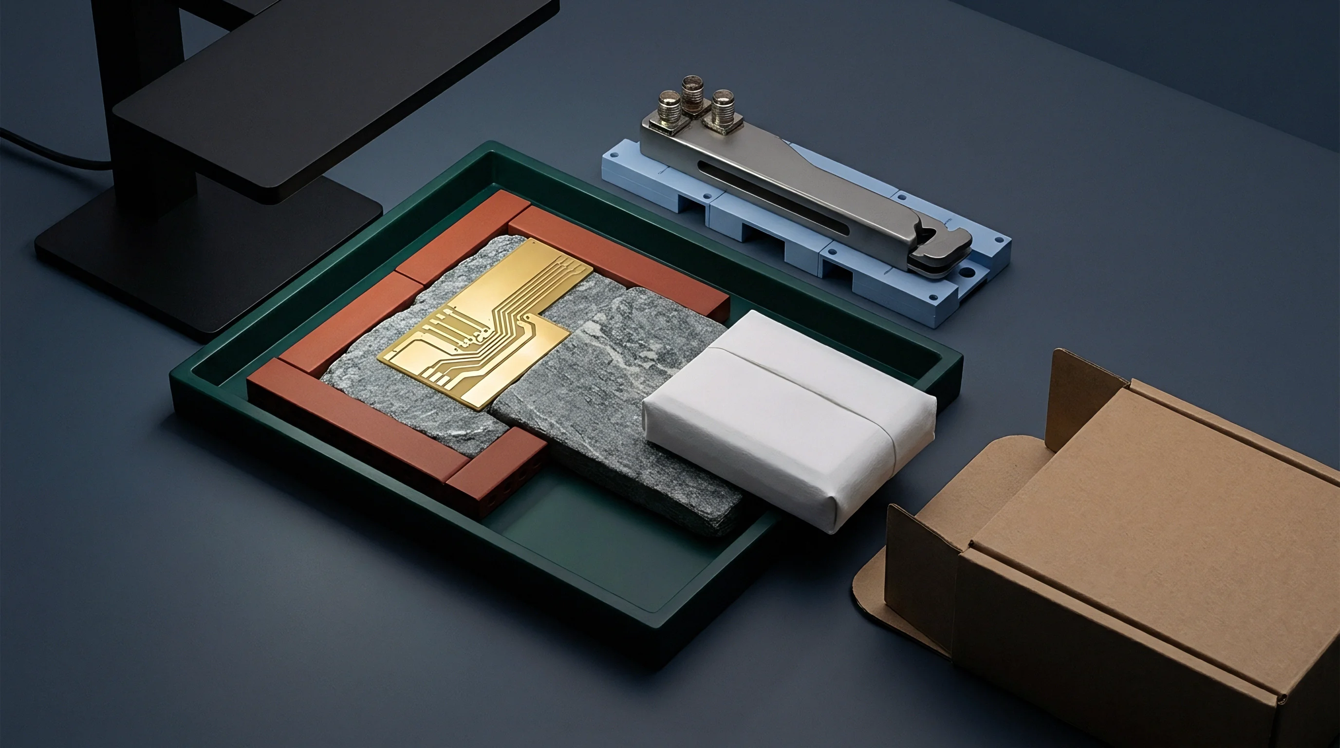
Probe
Quantifying sub-terahertz intermodulation products requires test architectures that isolate low-level mixing products from harmonic distortion in driving sources. Above 100 GHz, generating two independent high-power tones demands dedicated frequency multiplier chains, solid-state power amplifiers, and ultra-high-isolation directional couplers. Measuring intermodulation signals near -120 dBm in the presence of +20 dBm driving carriers requires careful bench design ~ including carrier suppression to protect the receiver LNA ~ to prevent spurious self-intermodulation inside the receivers.
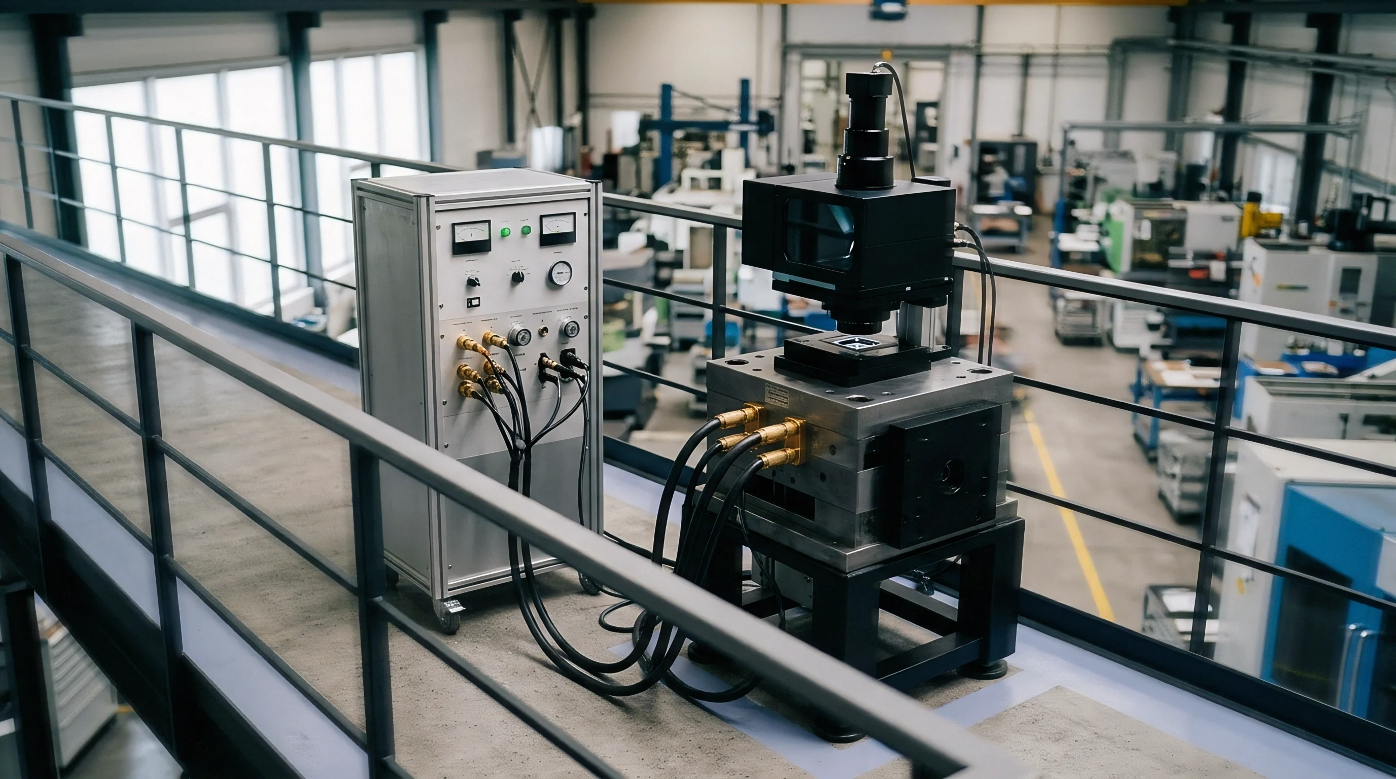
Dual-Tone Synthesizer Arrays and Carrier Cancellation Bridges
Sub-millimeter test setups combine two high-power source signals using low-loss directional couplers or diplexers. Because phase noise corrupts weak IM3 tones, drive signals f1 and f2 must carry high spectral purity to prevent transmitter phase noise from obscuring third-order intermodulation products (2f1 – f2). High-Q waveguide cavity notch filters or active vector cancellation bridges remove primary carrier power before the low-noise receiver front end, preventing mixer saturation and artificial intermodulation.
| Architecture Type | Dynamic Range (dB) | Carrier Isolation Method | Primary Limitation |
|---|---|---|---|
| Direct Waveguide Reflection | 85 ~ 95 | High-directivity directional coupler | Coupler internal non-linearity limits system floor |
| Active Carrier Cancellation Bridge | 110 ~ 125 | Vector phase and amplitude nulling | Requires continuous manual or automated feedback re-nulling |
| Quasi-Optical Transmission Test | 100 ~ 115 | Free-space frequency-selective surfaces | Requires high-power sources due to free-space path loss |
Compliance with IEEE 1785.2 requires verification of flange planar parallelism within 0.5 micrometers to prevent spurious micro-gap arc discharge during multi-carrier excitation.
Reflection measurements use a high-directivity waveguide coupler to sample backward-propagating intermodulation tones produced by the Device Under Test, while transmission setups evaluate tones passing through the flange interface into a terminated load. Failing to account for source multiplier harmonic self-mixing yields false passive intermodulation readings that can invalidate vendor qualification campaigns.


Arithmetic
Evaluating link degradation from flange passive intermodulation requires calculating the carrier-to-intermodulation ratio at the receiver front end. Sub-terahertz link budgets operate with narrow thermal noise margins, where even a minor intermodulation tone can degrade signal-to-noise ratio enough to trigger packet drops or force lower modulation orders.

Worked Link Budget Model for Sub-Terahertz Waveguide Interfaces
Consider a 220 GHz satellite feeder uplink using WR-4.3 waveguide interfaces operating at a nominal output power of +18 dBm per carrier, driven by two CW carriers (f1 = 220.0 GHz, f2 = 220.5 GHz). The flange interface under test exhibits a measured third-order intermodulation ratio (C/IM3) of -110 dBc at a reference drive level of +15 dBm per tone. Drive power scaling follows a 2:1 dB rule for third-order products: a 1 dB increase in carrier power increases intermodulation power by 3 dB, yielding a net 2 dB degradation in carrier-to-intermodulation ratio.
At +18 dBm input power per tone, the drive level rises +3 dB above reference. Absolute intermodulation tone power scales as:
PIM3 = PIM3, ref + 3 × (Pcarrier – Pref) = (-95 dBm) + 3 × (3 dB) = -86 dBm
In a transmission path with four cascaded flange joints between the power amplifier and feed horn, coherent voltage addition across all four interfaces represents the worst-case phase alignment. Coherent accumulation adds voltage linearly:
Δ Pcascade = 20 log10(Ninterfaces) = 20 log10(4) ≈ 12.04 dB
Total intermodulation power entering the receiver feed reaches -86 dBm + 12.04 dB = -73.96 dBm. If receiver thermal noise floor across a 500 MHz channel bandwidth sits at -90 dBm, the intermodulation tone exceeds that noise floor by 16.04 dB, severely degrading sensitivity and link margin.
To qualify flange performance on the test bench, operators follow a standardized calibration and measurement workflow:
- Set the primary tone power level to +15 dBm using precision rotary vane attenuators.
- Adjust tone spacing to match the receiver channel raster within the sub-terahertz operating band.
- Measure receiver noise floor with driving sources disabled to set the baseline thermal noise reference.
- Energize carriers and observe the third-order intermodulation tone on the spectrum analyzer.
- De-embed line losses and coupler directivity factors to determine the true intermodulation power at the flange interface.
Summing non-linear contributors across eight waveguide segments yields a closed-form prediction of total system signal degradation.

Clamp
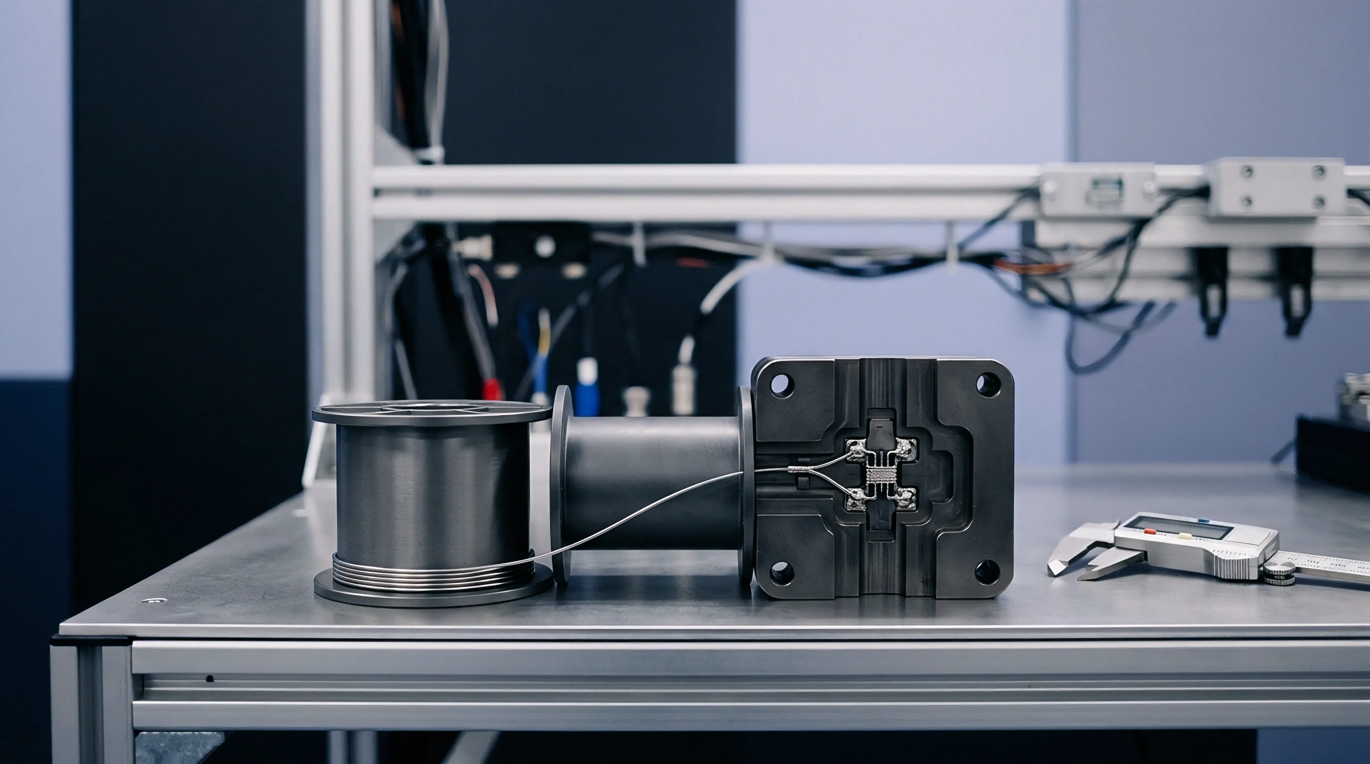
Securing sub-terahertz waveguide flanges requires uniform contact stress across the alignment face to prevent micro-gaps. Fastener torque dictates contact pressure, while thermal stress can distort flange flatness. Insufficient or uneven bolt clamping leaves microscopic air gaps between waveguide openings, sharply reducing contact pressure and accelerating non-linear mixing.

Fastener Torque and Surface Flatness Compliance
Precision UG-387/M modified flange standards use four 4-40 UNC stainless steel screws alongside dual dowel pins to constrain transverse shift. Tightening torque must reach 0.57 Nm (5.0 in-lbs) to achieve uniform metallic yield across the flange ring surface. Because fastener relaxation alters joint pressure, improper screw materials like soft brass or unpassivated carbon steel allow bolts to stretch over thermal cycles, relaxing contact stress.
Mechanical bolt relaxation over repeated thermal cycles creates microscopic surface separation that elevates passive intermodulation power.
Achieving stable electrical linearity across precision interfaces mandates strict adherence to physical assembly parameters:
- Alignment Pin Tolerances verify dowel pin fit within h6/m6 limits to guarantee repeatable transverse alignment within 2 micrometers.
- Torque Wrench Calibration verify screwdrivers apply precise torque within a 2 percent error window to avoid asymmetric stress distribution.
- Plating Thickness Verification inspect electroplated gold layer depth to maintain 0.8 to 1.2 micrometers thickness over dense nickel flash.
- Thermal Expansion Matching select hardware materials matching copper CTE to minimize interface movement during cryogenic or elevated temperature cycles.
While gold’s oxidation resistance prevents long-term drift, surface flatness must still stay below 0.5 micrometers total indicator reading across the sealing plane. Applying uniform star-pattern torque across flange bolts prevents localized gap deformation and stabilizes intermodulation across the interface.


Audit
Procuring mmWave and sub-terahertz front-end modules requires rigorous sourcing protocols to validate mechanical tolerances before accepting volume shipments. RFQ documentation must codify maximum allowable intermodulation levels under actual operating drive conditions, and factory qualification dossiers must present physical surface interferometry data alongside calibrated RF intermodulation test traces.

Contractual Specifications and Factory Acceptance Protocols
Commercial contracts for sub-terahertz radio hardware specify strict intermodulation thresholds under multi-tone drive conditions, requiring vendor compliance with IEEE 1785 specifications governing sub-millimeter waveguide interfaces. Procurement protocols mandate testing 100 percent of flight hardware or ground terminal feed networks on dual-tone high-power RF benches prior to shipment sign-off.
| Evaluation Parameter | Test Method | Acceptance Threshold | Commercial Penalty for Non-Compliance |
|---|---|---|---|
| Interface Surface Flatness | White-Light Interferometry | < 0.3 μm across entire flange face | Lot rejection and 100% vendor re-inspection fee |
| Third-Order PIM Power | Dual-Tone Bench Test (+15 dBm drive) | < -120 dBc at 140/220 GHz | Module rejection and vendor chargeback |
| Plating Adhesion & Purity | X-Ray Fluorescence (XRF) Scan | 99.9% pure Au, 0.8 ~ 1.2 μm depth | Refurbishment at vendor cost plus shipping line hold |
Failing to specify strict interface roughness standards in procurement documentation leads to high field failure rates and costly replacement programs. Standard procurement clause IEEE 1785.3-A4 mandates white-light interferometric surface topography verification for all production lots, shifting liability for non-linear interface distortion directly to the component manufacturer.