Intermetallic Diffusion Degradation Limits in High Frequency Pin Interfaces
Intermetallic growth at high frequency pin interfaces increases surface resistance and insertion loss, degrading RF link margin across multi-gigahertz modules.


Phase

Lattice Diffusion and Intermetallic Growth at High Frequency Contact Interfaces
Atomic migration between plating layers and underlying copper constructs distinct intermetallic crystalline phases across radio module pin contacts. Driven by chemical potential gradients, gold, tin, copper, and nickel atoms traverse boundary zones to assemble stoichiometric compounds including Cu6Sn5, Cu3Sn, AuSn4, and Ni3Sn4. Thermal exposure during SMT reflow and standard field operation supplies the activation energy for this exchange.
High-frequency headers, board-to-board interconnects, and castellated module pads depend on clean metallic boundaries to preserve low ohmic resistance and target characteristic impedances.
When tin-lead or lead-free tin finishes sit directly over raw or thinly plated copper, copper diffuses into the tin matrix even at room temperature. Growth begins with η-phase Cu6Sn5 right at the interface. Continued heat drives further copper migration into this layer, creating an adjacent ε-phase Cu3Sn band against the copper base.
Electrical resistivity rises sharply in these phases: pure copper measures 1.7 microhm-centimeters, while Cu6Sn5 sits at 17.5 microhm-centimeters and Cu3Sn at 8.9 microhm-centimeters. When pins use gold flash directly over copper or nickel, the gold dissolves into molten tin during reflow and precipitates as AuSn4 crystals, leaving a brittle boundary vulnerable to vibration-induced cleavage.

Protocol Margin Degradation across Wireless Frequency Bands
Intermetallic growth creates localized impedance discontinuities across surface-mount pins carrying RF energy. Higher bulk resistivity within this boundary layer increases ohmic insertion loss, eating into link margins established during design. In a 2.4 GHz Bluetooth Low Energy or IEEE 802.15.4 Zigbee design running +0 dBm output power against -93 dBm receiver sensitivity, a 1.5 dB drop across degrading pin joints pulls maximum line-of-sight range from 100 meters down below 84 meters.
In sub-GHz LoRaWAN links at 868 MHz or 915 MHz, where 148 dB budgets cover several kilometers in city environments, intermetallic buildup detunes matching networks, inducing return loss mismatches that pull down total radiated power.
High-density cellular modules running LTE-M and NB-IoT run hot at the RF pins during sustained uplink bursts in fringe coverage. Power amplifier currents pushing pin temperatures to 85°C double diffusion rates compared to a 25°C baseline, thickening the boundary zone over 1,000 operating hours. This shift raises the voltage standing wave ratio from 1.2:1 to past 2.1:1, forcing power amplifier current foldback and cutting active transmission rates.
Plating thickness boundaries define whether solid-state atomic diffusion generates unstable stoichiometric intermetallics or preserves clean signal conduction across multi-gigahertz transitions.
Failure Modes Driven by Boundary Stoichiometry
Intermetallic growth reshapes the electrical and physical profile of high-frequency pin joints, with most structural failures tracing back to lattice volume shifts and unequal atomic diffusion.
- Kirkendall Voiding forms sub-micron cavities at the Cu3Sn to copper interface because copper atoms diffuse into the intermetallic matrix faster than tin atoms migrate backward, creating acoustic discontinuities that reflect gigahertz signal waves.
- Gold Embrittlement occurs when gold content in tin solder joints exceeds 3 percent by weight, precipitating coarse AuSn4 needles that cause mechanical shear under mechanical shock.
- Subsurface Oxidation develops when thin nickel barrier layers fail, allowing copper to migrate to the pin surface where atmospheric oxygen creates high-resistance copper oxides.
- Impedance Mismatching arises as high-resistivity intermetallic layers thicken, shifting the effective dielectric and conductive geometry of microstrip-to-pin transitions.
Factory screening often shows normal DC continuity across tarnished pins and minor intermetallic boundaries, but high-frequency currents remain confined by skin depth to the outermost surface layers where these compounds concentrate.


Depth

Skin Depth Mechanics in Intermetallic Conductor Layers
Alternating current density drops off exponentially from a conductor’s surface toward its core as signal frequency climbs. The skin depth marks the point where current density falls to 1/e, roughly 37 percent of its surface peak. While direct current traverses the entire pin cross-section, gigahertz-band signals are forced into a thin outer perimeter by electromagnetic fields.
This depth is governed by frequency, magnetic permeability, and bulk resistivity. In pure copper, skin depth is 2.06 microns at 1 GHz, tightening to 1.33 microns at 2.4 GHz, 0.86 microns at 5.8 GHz, and 0.42 microns at 24 GHz. When intermetallics like Cu6Sn5 displace clean copper along this boundary, higher resistivity widens the physical skin depth while driving up surface resistance.
Because current is forced through resistive intermetallic phases instead of copper, RF conductor losses scale directly with layer growth.
| Material Phase | Resistivity (μΩ·cm) | Skin Depth at 900 MHz (μm) | Skin Depth at 2.4 GHz (μm) | Skin Depth at 5.8 GHz (μm) |
|---|---|---|---|---|
| Pure Copper (Cu) | 1.71 | 2.19 | 1.34 | 0.86 |
| Pure Gold (Au) | 2.44 | 2.62 | 1.60 | 1.03 |
| Pure Nickel (Ni) | 6.99 | 0.70 | 0.43 | 0.28 |
| Cu6Sn5 Intermetallic | 17.50 | 7.02 | 4.30 | 2.77 |
| Cu3Sn Intermetallic | 8.90 | 5.01 | 3.07 | 1.97 |
| AuSn4 Intermetallic | 34.00 | 9.78 | 5.99 | 3.86 |

RF Loss Amplification in Thin Conductor Geometries
Signal attenuation accelerates when intermetallic growth reaches or exceeds the operational skin depth. On a fresh castellated pad with 1.0 micron of gold over nickel, current travels mostly within the clean outer shell. Following thermal exposure, diffusion can convert the outer 2.5 microns into mixed AuSn4 and Ni3Sn4 intermetallics.
At 5.8 GHz, where clean gold has a skin depth of 1.03 microns, the entire active signal path falls inside this transformed zone.
Increased surface resistance lowers the quality factor of matching networks and filter geometries built into the module launch. The resulting series resistance raises insertion loss along standard attenuation curves: an interface logging 0.05 dB loss at 2.4 GHz can degrade to 0.45 dB once Cu6Sn5 spans the full skin depth. In Wi-Fi 6E hardware running 6 GHz, where 1024-QAM requires a minimum 35 dB signal-to-noise ratio, this loss spikes packet error rates, prompting rate downshifts and strangling throughput.
At frequencies above 5 GHz, current flow concentrates entirely within the first micron of the conductor surface, turning microscopic intermetallic growth into a primary source of RF signal attenuation.
Why Does Gold Migration Accelerate High Frequency Attenuation under Thermal Load?
Gold stops oxidation during shelf storage, but thin flash layers dissolve into molten tin-lead or SAC300 solders in seconds during reflow. This dissolved gold disperses into the liquid solder joint. As it solidifies, gold precipitates out as AuSn4 crystals grouped against the copper or nickel pad wall.
Under extended thermal bias during operation, residual gold in the flash coating continues migrating into solid tin along grain boundaries. This solid-state diffusion forms continuous AuSn4 films across high-frequency conduction paths. With a bulk resistivity of 34 microhm-centimeters ~ roughly twenty times that of copper ~ a continuous AuSn4 layer within the skin depth creates an electrical bottleneck that dissipates RF energy as heat and cuts radiated output at the antenna feed.
A simple rule of thumb holds that whenever intermetallic growth thickness exceeds one half of the operational skin depth, high-frequency attenuation increases beyond acceptable link budget tolerances.


Barrier

Ni, Pd, and TiW Underplate Stackups and Stoichiometric Suppression
Curbing atomic diffusion between copper pins and exterior tin plating requires an underplate barrier. Electroless or electrolytic nickel remains standard here; nickel reacts far more sluggishly with tin than copper does, producing Ni3Sn4 at a fraction of the Cu6Sn5 growth rate. A solid nickel barrier keeps copper from reaching the outer perimeter, preserving mechanical fit and electrical behavior over long operating spans.
Harsh-environment military and industrial radios often use palladium or titanium-tungsten (TiW) thin-film stacks beneath gold or tin finishes. Depositing 0.1 to 0.2 microns of palladium over 2.0 to 4.0 microns of nickel builds a dual-layer barrier: palladium stops nickel oxidation prior to assembly, while the nickel substrate pins copper in place. On ceramic radio substrates, a sputtered 0.05-micron titanium-tungsten layer provides diffusion suppression up to 300°C, holding off gold and copper migration across transmission lines.
| Barrier Architecture | Activation Energy (eV) | Growth Rate at 85°C (μm/√hr) | Growth Rate at 125°C (μm/√hr) | Thermal Stability Threshold (°C) |
|---|---|---|---|---|
| Bare Cu to Sn Interface | 0.68 | 0.0120 | 0.0450 | 60 |
| Electrolytic Ni (2.0 μm) | 1.15 | 0.0008 | 0.0035 | 150 |
| Electroless Ni-P (7% P) | 1.28 | 0.0004 | 0.0019 | 175 |
| Ni/Pd Stackup (3.0 μm / 0.15 μm) | 1.32 | 0.0003 | 0.0014 | 200 |
| Sputtered TiW (0.08 μm) | 1.85 | 0.00001 | 0.0001 | 300 |

Stoichiometric Boundaries and Plating Process Control
Electroless nickel baths introduce phosphorus via sodium hypophosphite reducing agents, and phosphorus concentration determines the deposit’s crystalline structure. Low-phosphorus baths (2 to 5 percent P) yield microcrystalline deposits full of grain boundaries that encourage diffusion. Mid-phosphorus (6 to 9 percent P) and high-phosphorus (10 to 13 percent P) chemistries produce amorphous layers free of grain boundaries, cutting intermetallic formation rates tenfold.
Soldering or heating causes tin to react with electroless nickel-phosphorus, drawing nickel into Ni3Sn4. Phosphorus is rejected by the Ni3Sn4 lattice, accumulating instead at the reaction front as a phosphorus-rich Ni3P layer. Left unchecked, this Ni3P phase produces brittle micro-voids under cyclic strain.
Maintaining nickel depth above 3.0 microns with phosphorus tightly bounded between 7 and 9 percent provides diffusion resistance without risking embrittlement.
Amorphous electroless nickel coatings containing eight percent phosphorus eliminate crystalline grain boundaries, slowing atomic diffusion by ninety percent relative to pure copper substrates.

Barrier Specification Checklist for Module Procurement
Procurement specifications require verifiable parameters for pin plating stacks, which receiving audits can validate directly.
- Minimum Nickel Underplate Depth mandates a continuous electrolytic or electroless nickel layer measuring no less than 3.0 microns across all contact faces.
- Phosphorus Composition Windows establish strict chemistry bounds between 7.0 and 9.0 percent phosphorus weight ratio in electroless nickel baths.
- Gold Flash Thickness Ceilings cap soft or hard gold immersion layers at 0.05 microns to prevent gold embrittlement in lead-free solder joints.
- Intermetallic Barrier Verification Standards specify test protocols using cross-sectional scanning electron microscopy and energy-dispersive X-ray spectroscopy to confirm layer continuity.
Under IPC-A-610 Class 3 standards for high-reliability electronics, any pin interface exhibiting continuous copper-to-tin intermetallic growth exceeding 1.5 microns prior to environmental screening triggers immediate lot rejection.

Fatigue
Thermal Cycling, Microvoiding, and Stress Creep
Thermal cycling generates cyclic stresses across contact interfaces due to CTE mismatches between circuit boards, ceramic substrates, and copper pins. Standard FR-4 moves at 14 to 17 ppm/°C in the X-Y plane, ceramic packages expand at 6 to 8 ppm/°C, and copper pins sit between them at 16.5 ppm/°C. Shifts between outdoor lows of -40°C and internal operating peaks of +85°C impose persistent shear strains on solder joints.
These strains accelerate diffusion via stress-assisted mechanisms. Hydrostatic tension near intermetallic boundaries lowers the barrier for vacancy movement. Unbalanced diffusion fluxes cause vacancies to pool at stress points, forming Kirkendall voids.
Across hundreds of thermal cycles, these voids merge into cracks running parallel to the contact interface, increasing resistance and producing transient signal dropouts.

Fretting Corrosion in Demountable Pin Interfaces
Demountable RF contacts, including spring pins and stamped socket headers, suffer micro-motions driven by thermal swings and mechanical vibration. Displacements of only 0.5 to 20 microns strip protective surface oxides and soft coatings. This fretting motion continually exposes bare metal to oxidation, building up fine oxide debris within the contact zone.
If intermetallic compounds have consumed the plating, wear exposes brittle sub-layers to ambient air. Cu6Sn5 and Ni3Sn4 oxidize quickly, generating non-conductive particulate that settles between contact surfaces. Contact force also declines as springs take a set at high operating temperatures.
When normal force slips below 30 grams, the interface no longer wipes away debris during engagement, causing RF contact resistance to climb from milliohms into hundreds of ohms.
A step-by-step stress verification procedure quantifies mechanical and intermetallic integrity across temperature profiles:
- Mount ten test samples onto production-grade evaluation boards using standardized SMT reflow profiles.
- Log baseline RF insertion loss and return loss from 100 MHz to 10 GHz using a calibrated vector network analyzer.
- Subject the assemblies to 500 thermal cycles from -40°C to +125°C with 15-minute dwell times per thermal extreme in a dual-chamber environmental chamber.
- Measure high-frequency signal transmission parameters at intervals of 100 cycles without disturbing the mechanical fixtures.
- Perform cross-sectional polish and scanning electron microscopy to measure intermetallic thickness and void density along the critical RF conductor paths.
What safety margin remains when high-density array modules undergo simultaneous thermal cycling and sustained random vibration during automotive extended testing?

Probe
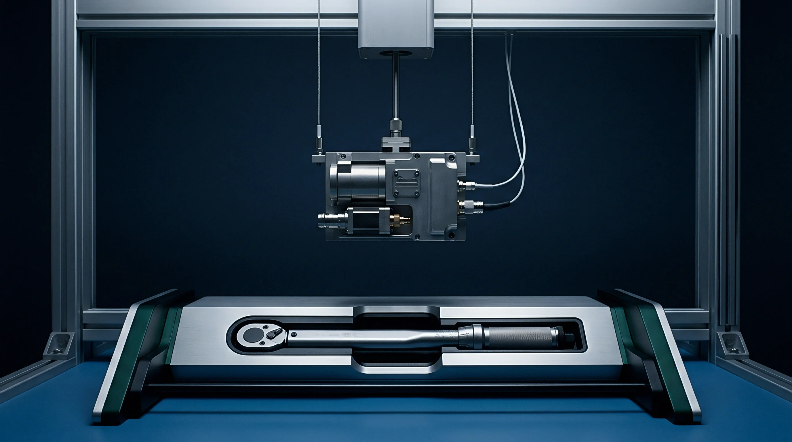
Bench Testing and Microstructural Diagnostics
Tracking intermetallic growth requires combining high-frequency s-parameter measurements with microstructural analysis. Direct-current resistance checks cannot isolate thin intermetallic growth layers because DC current flows through the bulk cross-section of the pin, masking microscopic high-resistance surface layers. RF network analyzer measurements identify localized surface degradation by detecting subtle increases in s-parameter insertion loss (S21) and shifts in reflection coefficients (S11).
Structural verification requires cross-sectional metallography. Samples are potted in epoxy, cut with diamond blades, and polished with alumina slurries down to 0.05 microns. Etching with ammonium hydroxide and hydrogen peroxide highlights grain boundaries and intermetallic bands under scanning electron microscopy.
Energy-dispersive X-ray spectroscopy then resolves elemental distributions, mapping the stoichiometry of Cu6Sn5, Cu3Sn, and Ni3Sn4 at sub-micron scales.
| Diagnostic Tool | Measurement Target | Resolution Limit | Destructive Test |
|---|---|---|---|
| Vector Network Analyzer | RF Insertion Loss & Return Loss | 0.01 dB at 10 GHz | No |
| 4-Wire Kelvin Probe | Bulk DC Contact Resistance | 10 microhms | No |
| Scanning Electron Microscopy | Intermetallic Layer Depth | 10 nanometers | Yes |
| Energy-Dispersive X-Ray | Stoichiometric Composition | 0.1 atomic percent | Yes |
| X-Ray Micro-CT Spectroscopy | Internal Subsurface Voiding | 1.0 micron | No |

High-Temperature Operating Life Verification Protocols
High-Temperature Operating Life (HTOL) tests drive intermetallic reactions by holding assemblies at elevated temperatures while running active RF signals through the pins. Common test profiles run at 105°C or 125°C for 1,000 continuous hours at maximum output power. Arrhenius models then allow engineers to project 1,000-hour performance at 125°C out to field lifespans exceeding 10 years at a normal 55°C baseline.
High-duty-cycle equipment ~ such as commercial Wi-Fi access points or cellular gateways handling continuous uplink data ~ shows accelerated pin degradation during HTOL testing. Ongoing RF currents induce localized Joule heating, pushing contact points 10°C to 15°C above the surrounding chamber air. This added heat speeds diffusion within the active skin depth, leading to early link margin loss.
High-Temperature Operating Life tests that omit active RF power transmission fail to replicate localized Joule heating, underestimating field diffusion rates by up to forty percent.
Dossier Requirements for Interface Qualification
Verifying plating stacks requires comprehensive engineering dossiers before issuing volume production commitments. A complete qualification package covers several chemical and structural proofs.
- Cross-Sectional SEM Micrographs providing 5,000x magnification images of pin plating interfaces before and after 1,000-hour thermal stress exposure.
- Elemental Composition Maps documenting nickel barrier integrity and confirming zero copper migration to the outer tin surface.
- S-Parameter Attenuation Profiles tracking RF insertion loss shifts across target operating frequency bands through thermal cycling milestones.
- Plating Thickness Audit Certificates confirming compliance with minimum nickel and maximum gold immersion parameters for every production lot.
Bypassing SEM cross-sections during qualification lets latent plating flaws pass into volume production, risking field failures once intermetallics degrade link ranges after a year in service.


Invoice
Landed Cost Effects of Plating Stackups and Yield Losses
Plating stackup decisions feed directly into module pricing, yield rates, and total landed cost. Raw copper pins with simple immersion tin represent the lowest unit purchase cost, shaving $0.03 to $0.06 per module compared to barrier-plated options. That initial saving carries field liabilities: bare copper-tin interfaces diffuse during storage, dropping solderable shelf life from twelve months to under ninety days.
Adding an electrolytic nickel barrier with gold flash raises module costs by $0.08 to $0.14, varying with metal markets. Across 100,000 sub-GHz smart meter modules, this stack adds $12,000 to upfront bill-of-materials costs. That expense offsets link degradation and protects against site visits averaging over $150 each when deployed units lose signal at the antenna pin.

Commercial RFQ Specifications and Warranty Protections
Procurement teams drafting RFQs for RF modules incorporate strict metallization specifications to guard against thin plating. Relying on basic datasheets provides little recourse once intermetallic degradation triggers field drops outside 90-day receiving windows. Detailed plating controls embedded in procurement contracts oblige suppliers to carry warranty costs tied to interface failures.
Strong procurement agreements link milestone disbursements to microstructural audit reports from independent laboratories. Typical terms require suppliers to warranty a 10-year service life at 85°C junction conditions with under 0.5 dB RF insertion loss drift at operating frequencies. Defining barrier thicknesses, bath chemistry targets, and HTOL schedules shifts risk back to the supplier, ensuring consistency across volume production runs.
Product warranties specifying zero performance drift over five years remain unenforceable unless incoming batch inspection plans verify nickel barrier thickness on every plating lot before SMT assembly.