Closed-Loop Antenna Vector Impedance Sensor Integration and Calibration Mechanics
Closed-loop vector impedance sensing restores transmitter efficiency by adjusting tunable matching networks to neutralize antenna detuning under field conditions.
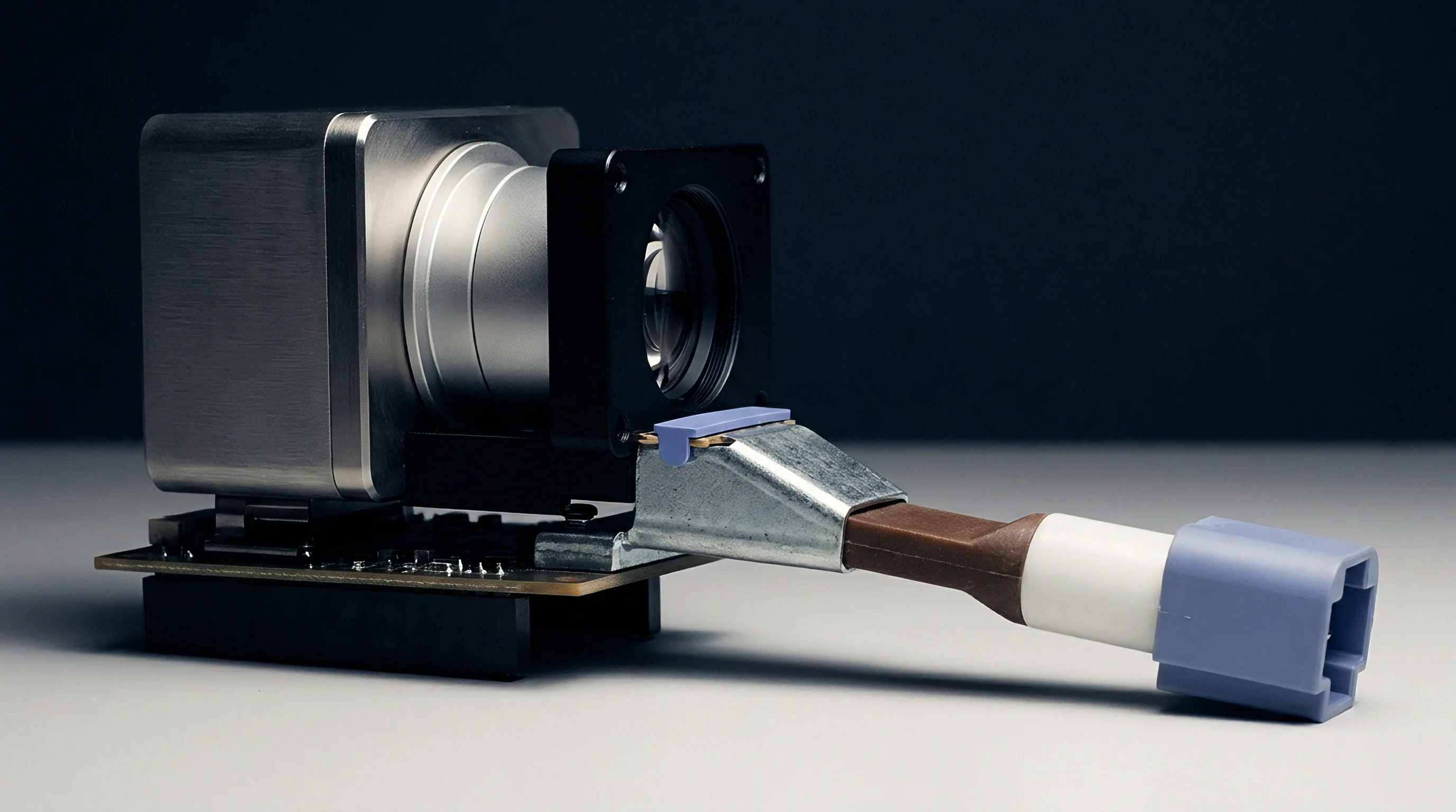

Bridge
Integrated radio frequency front ends require precise real-time measurement of the complex reflection coefficient presented by an antenna. Transmitted energy traveling toward an uncalibrated or detuned radiating element generates a reflected wave, setting up a voltage standing wave along the feedline. Traditional scalar detectors measure only the magnitude of this reflection, leaving the phase angle unknown.
Closed-loop vector impedance sensing resolves both magnitude and phase, providing the complete complex scattering parameter S11 required to synthesize a conjugate match. The underlying sensing architecture uses coupled lines or balanced resistive nodes inserted between the power amplifier output and the matching network input.

Integrated Directional Couplers and Resistive Detection Topologies
RF front-end designers select sensing structures based on board area constraints, operating bandwidth, and permissible insertion loss. Dual-directional microstrip or strip-line couplers isolate forward and reverse power waves through magnetic and electric field sampling. These passive structures deliver high directivity, preventing forward power from corrupting the reverse wave measurement.
Physical trace length scales inversely with frequency, rendering coupled-line structures large at sub-gigahertz allocations. Resistive sensing topologies bypass physical length limitations by creating a balanced bridge on silicon or low-temperature co-fired ceramic substrates. Directivity sets the measurement floor.
When directivity drops below 20 dB, the reverse voltage sample absorbs parasitic energy from the forward wave. This leakage distorts the calculated complex reflection coefficient, introducing phase errors that propagate into the tuning algorithm. High insertion loss directly lowers transmitter margin.
Insertion loss across the sensing element subtracts from the total power delivered to the radiating element, forcing the power amplifier to draw additional DC current to maintain total radiated power targets.
| Sensing Topology | Bandwidth Range | Directivity (dB) | Insertion Loss (dB) | Silicon Area (mm²) |
|---|---|---|---|---|
| Dual Microstrip Coupler | 1.7 GHz to 6.0 GHz | 22 to 28 | 0.15 to 0.30 | 12.50 to 25.00 |
| Integrated Resistive Bridge | 0.4 GHz to 3.8 GHz | 14 to 20 | 0.40 to 0.75 | 0.85 to 1.50 |
| Transformer-Based Hybrid | 0.7 GHz to 2.7 GHz | 18 to 24 | 0.25 to 0.45 | 2.10 to 4.20 |
| Capacitive-Voltage Current Probe | 2.4 GHz to 7.1 GHz | 12 to 16 | 0.10 to 0.20 | 0.45 to 0.90 |

Magnitude and Phase Vector Extraction Mechanics
Down-converting sampled forward and reverse RF signals into baseband in-phase and quadrature components yields the complex reflection magnitude and phase angle. Monolithic gain and phase detectors process the RF samples through matched logarithmic amplifiers, outputting analog voltages proportional to the log ratio of reverse to forward amplitude and the relative phase difference. Advanced integrated transceivers route forward and reverse samples directly into quadrature mixers driven by the main local oscillator, generating analog baseband base vectors.
Analog-to-digital converters convert these signals into raw digital complex pairs.
Raw digital pairs contain continuous systematic errors induced by trace length asymmetries, mixer offset voltages, and component tolerances across operating temperature ranges. High standing waves stress power amplifiers. Uncorrected raw phase measurements cause tuning algorithms to execute impedance adjustments in incorrect quadrants of the Smith chart.
Factory calibration eliminates these systematic vector distortions by mapping raw sensor outputs against known impedance standards.
Silicon suppliers routinely claim sensor measurement accuracy without accounting for board-level trace coupling or housing dielectrics, leaving module integrators to resolve real-world vector offset errors independently during final assembly qualification.


Mismatch
Antenna structures in handheld, wearable, and industrial wireless enclosures experience severe environmental detuning during operational cycles. Near-field interactions with human tissue, conductive enclosures, metallic mounting surfaces, and adjacent battery packs alter the boundary conditions governing electromagnetic radiation. The free-space resonant frequency shifts, forcing the complex impedance away from the nominal 50-ohm reference value toward edge regions of the Smith chart.
Uncorrected impedance shifts degrade the total active reflection coefficient, causing power amplifier efficiency drops, harmonic distortion growth, and link budget erosion.

Dielectric Loading and Environmental Detuning Dynamics
Human skin and high-permittivity plastics introduce dielectric loading that increases the effective electrical length of an antenna. Higher electrical length lowers the fundamental resonant frequency. In a 2.4 GHz Wi-Fi or Bluetooth Low Energy device operating under IEEE 802.11b/g/n or IEEE 802.15.4 standards, hand placement shifts the primary resonance downward by 150 MHz to 400 MHz.
Dielectric loading shifts resonance downward. This frequency shift changes the load impedance seen by the RF front end from a purely real 50 ohms to a complex load with high reactive reactance and reduced real resistance.
The total radiated power drops by 4.2 dB when an antenna with a 2.15 dBi gain at 2.44 GHz experiences a complex load shift from 50 ohms to 12 – j38 ohms under human hand contact.
Sub-gigahertz allocations, such as 868 MHz and 915 MHz LoRaWAN or Long Term Evolution for Machines bands, exhibit severe reactive shifts due to their larger near-field boundary zone. A metallic structure brought within a quarter-wavelength creates inductive or capacitive coupling, altering the current distribution across the radiating element. Unchecked reflections reduce battery runtime.
The standing wave ratio climbs from an acceptable 1.2:1 up to 6.0:1 or higher, reflecting more than 50 percent of transmitted RF energy back into the transmitter output port.

Power Amplifier Degradation under Severe Reflection
Solid-state RF power amplifiers operate with optimal load lines designed to maximize output power and power-added efficiency while maintaining spectral mask compliance. Deviations from the optimal load impedance distort the dynamic load line, forcing the output transistor into saturation or excessive voltage breakdown regimes. Inductive mismatches generate voltage spikes that exceed the drain-to-source breakdown voltage, degrading junction reliability over time.
Capacitive mismatches force high peak currents through the channel, producing excessive thermal dissipation.
- Thermal Junction Degradation occurs when persistent high standing wave ratios concentrate dissipation inside the transistor channel, increasing thermal resistance and accelerating silicon wear.
- Spectral Mask Violations emerge as severe load shifts alter transistor non-linear dynamics, elevating adjacent channel leakage ratios beyond ETSI EN 300 328 and FCC Part 15 limits.
- Transmitter Efficiency Loss scales directly with reflected power, converting battery energy into dissipated thermal dissipation rather than radiated electromagnetic energy.
- Receive Chain Desensitization happens when mismatched transmit signals leak across front-end switches into low-noise amplifiers, elevating the receiver noise floor.
Failure to correct high voltage standing wave ratios permanently degrades transmitter efficiency, forcing power amplifiers into thermal throttling and causing premature battery exhaustion in low-power industrial end nodes.


Loop
Adaptive impedance matching relies on digital control routines operating within closed-loop feedback frameworks to drive tunable components. Digital tunable capacitors based on Silicon-on-Insulator technology or micro-electro-mechanical switches form Pi, T, or L-type matching networks between the power amplifier and the antenna. The control algorithm samples the complex reflection coefficient from the vector sensor, computes the impedance error relative to the 50-ohm center, and commands switch states to move the transformed load impedance toward the conjugate match.
Tuning algorithms require bounded search spaces.

Iterative Search and Matrix Lookup Control Mechanics
Gradient descent control routines evaluate real-time vector impedance gradients, shifting matching capacitor values incrementally to locate local reflection minima. Gradient descent excels under smooth impedance transitions but struggles with local minima created by highly reactive load topologies. Fast lookup table algorithms match measured complex vectors directly against pre-computed impedance transformation matrices.
Direct matrix transformation computes optimum capacitor switch combinations in a single algorithmic pass, reducing convergence latency.
| Control Algorithm | Convergence Speed (µs) | DC Power Draw (mW) | Memory Footprint (kB) | Stability Margin (dB) |
|---|---|---|---|---|
| Steepest Gradient Descent | 120 to 450 | 1.2 to 2.4 | 4.5 to 8.0 | 12 to 18 |
| Direct Matrix Lookup | 15 to 40 | 0.4 to 0.8 | 32.0 to 64.0 | 8 to 14 |
| Coordinated Nelder-Mead Simplex | 250 to 800 | 2.1 to 4.2 | 12.0 to 24.0 | 15 to 22 |
| Adaptive Neural Mapping | 50 to 110 | 3.5 to 6.8 | 128.0 to 256.0 | 10 to 16 |
Algorithmic execution speed must match the operational frame structures of targeted radio protocols. Cellular LTE-M and NB-IoT protocols enforce rigid subframe timing that demands impedance convergence within time-slot guard bands to prevent packet corruption. Wi-Fi 6 systems operating across 2.4 GHz and 5 GHz channels require rapid re-tuning during channel sounding sequences.
Active tuning consumes discrete energy packets.
Matching network tuning routines must finalize switch state changes during packet preamble transmission to prevent amplitude modulation distortion across payload symbols.

Digital Tunable Capacitor Execution and Settling Dynamics
State changes inside Silicon-on-Insulator digital tunable capacitors involve switching arrays of microscopic high-voltage field-effect transistors that connect discrete metal-insulator-metal capacitive elements. Electrostatic discharge protection networks and internal charge pumps supply gate voltages between 10 V and 30 V to hold switch state linearity under 30 dBm RF voltage swings. Switching operations generate brief control line transients and capacitive ring-down oscillations that must settle before the vector sensor samples the newly transformed impedance state.
- Sample forward and reverse RF vector coupling signals at the directional sensor output during transmit burst initialization.
- Digitize phase and magnitude analog voltages through synchronized high-speed sampling analog-to-digital converters.
- Calculate raw load reflection parameters and apply factory temperature-compensation matrix offsets.
- Determine the optimal capacitor switch vector using the direct matrix lookup routine stored in local flash memory.
- Transmit SPI or MIPI Radio Frequency Front End control words to update digital tunable capacitor switch states.
- Wait for charge pump stabilization and switch capacitive settling cycles to finalize.
- Re-sample reflection vectors to verify return loss exceeds the 15 dB threshold.
Phase plane rotation alters impedance trajectory. Quantized capacitor steps limit impedance resolution. Selecting component switch settings based on coarse grid points leaves residual reactive impedance, which prevents the front end from reaching a true 50-ohm conjugate state.
A closed-loop impedance control algorithm that updates switch states faster than the physical component settling time will generate continuous limit-cycle oscillations across the matching network.


Matrix
Raw vector sensor readings deviate from true RF impedance values due to systematic losses, physical trace asymmetries, capacitive pad parasitics, and component phase shifts. Factory calibration establishes systematic error correction matrices by executing Short-Open-Load-Thru calibration procedures on automated test benches. Calibration transforms raw sensor outputs into precise complex scattering parameters referenced directly to the antenna interface plane.
Thermal expansion alters PCB trace capacitance.

Factory Vector Calibration and Systematic Error Removal
Single-port vector impedance sensor calibration adapts the classic twelve-term vector network analyzer error model into a streamlined three-term error matrix comprising directivity, source match, and reflection tracking. Factory test fixtures present known precision impedance standards to the module antenna pin during production testing. Short, Open, and 50-ohm Load standards generate three distinct raw complex voltage vectors that resolve the linear system of equations governing systemic error terms.
Precision calibration accounts for board dielectric variations and component soldering tolerances. Sensor performance degrades when operating junction temperatures depart from ambient factory calibration points. Silicon directional bridges and logarithmic detectors possess temperature-dependent gain and phase drift profiles.
Calibration records store multi-point temperature offset coefficients within module non-volatile memory, enabling the internal microcontroller to continuously update error correction matrices using real-time temperature sensor telemetry.
The list below details the structural documentation elements required within an RF module factory calibration docket to ensure compliance across production batches.
- Standard Calibration Reference File contains raw complex voltage vectors acquired from precision 50-ohm, open, and short calibration loads across target operating frequencies.
- Thermal Drift Matrix Table documents Phase and Magnitude sensor voltage shifts measured across temperature steps from -40 degrees Celsius to +85 degrees Celsius.
- S-Parameter Vector Transformation Limits defines acceptable numerical boundaries for directivity, source match, and tracking error terms before flagging module failure.
- Matching Component Nominal Offset Table maps initial digital tunable capacitor states against baseline 50-ohm reference measurements to eliminate component tolerance stack-ups.

Where Does Phase Ambiguity Disrupt Adaptive Impedance Correction?
Phase ambiguity emerges when high standing wave ratios shift the phase angle of the complex reflection coefficient across boundaries where the sensor resolution degrades. Resistive sensing bridges and scalar-derived phase extraction circuits experience mathematical singularities when reflection phase approaches 0 degrees or 180 degrees. At these phase boundary states, small changes in raw sensor output produce large changes in calculated load reactance, leading to incorrect tuning vectors.
Near phase singularities, small measurement noise spikes skew vector calculations, sending switch control instructions into incorrect Smith chart regions. Dual-quadrature sensing blocks resolve this issue by processing both in-phase and quadrature components simultaneously, preserving phase linear accuracy across all 360 degrees of rotation. Vector feedback restores radiated carrier strength.
Correct calibration matrices maintain phase linearity, ensuring stability regardless of load reflection angle.
Standard qualification procedures specified in IEEE 802.15.4 specifications require module vendors to declare complex reflection measurement accuracy across all four Smith chart quadrants under operating temperatures spanning -40 degrees Celsius to +85 degrees Celsius.


Audit
Integrating closed-loop antenna tuning systems alters standard RF verification methodologies and impacts module manufacturing economics. Automated test equipment must validate closed-loop tuning dynamics under active radiated load pull conditions, exceeding simple 50-ohm conductive test protocols. Verification procedures quantify Total Radiated Power and Total Isotropic Sensitivity recovery across detuned load conditions, proving system performance in real-world application environments.

Conductive and Radiated Verification Protocols
Conductive testing measures front-end performance by attaching programmable RF load pull tuners to the module antenna port. The load tuner sweeps complex reflection states across voltage standing wave ratio circles from 1.5:1 to 6.0:1, covering all phase angles in 15-degree increments. Automated test scripts verify that the closed-loop controller detects detuning, executes matching adjustments, and restores return loss to values exceeding 12 dB within allocated time windows.
Radiated verification takes place inside anechoic chambers equipped with programmable liquid dielectric phantom bodies. Real-time power monitoring evaluates carrier restoration while human hand models touch the device enclosure. Radiated tests confirm that adaptive tuning recovers lost link margin without generating out-of-band harmonic spikes that violate regulatory compliance standards.
| Antenna Impedance State | Unadjusted TRP (dBm) | Closed-Loop TRP (dBm) | Unadjusted TIS (dBm) | Closed-Loop TIS (dBm) |
|---|---|---|---|---|
| Nominal (50 + j0 Ω) | +23.0 | +22.6 | -104.0 | -103.8 |
| Detuned (20 – j35 Ω) | +16.2 | +21.8 | -95.5 | -102.1 |
| Detuned (15 + j40 Ω) | +15.8 | +21.5 | -94.2 | -101.8 |
| Severe Detuning (8 – j60 Ω) | +11.1 | +19.4 | -88.0 | -98.5 |

Commercial Yield and Module Landed Cost Arithmetic
Adding closed-loop vector impedance sensing hardware increases the silicon dielectric footprint and total bill of materials cost. A discrete implementation featuring a directional coupler, IQ detector, digital tunable capacitors, and high-voltage charge pumps adds approximately 0.45 to 0.85 USD to the module hardware bill of materials. Fully integrated System-in-Package radios absorb these functions into main transceiver dies, reducing incremental component costs down to 0.18 to 0.35 USD at scale.
Harmonic radiation spikes under severe mismatch. Hardware cost increases are balanced by operational yield improvements and performance advantages. Radios with closed-loop tuning maintain link integrity under severe detuning, reducing device return rates caused by drop-outs in field deployments.
Higher manufacturing test yield stems from the system self-compensating for component tolerances, allowing looser initial production tolerances for printed circuit antenna traces.
Total landed cost calculations balance silicon component additions against battery capacity reductions. Closed-loop tuning restores transmitter efficiency, enabling product designs to shrink battery sizing while maintaining operational lifespans. Lower battery capacity requirements reduce shipping weight and cell costs, offsetting front-end sensing silicon investments.