Quantitative Risk Allocation Mechanisms for Unannounced Silicon Revisions in Multijurisdictional Radio Sourcing Contracts
Parametric contract clauses allocate unannounced silicon revision risks by linking physical RF and current draw deltas directly to invoice price reductions.


Silicon
Transceiver foundries alter mask sets to optimize wafer yield without altering external package markings. Integrated radio frequency systems-on-chip contain complex analog front-ends, baseband digital signal processors, embedded power management units, and integrated ROM microcode. Semiconductor foundries routinely implement die steppings, metal layer revisions, mask alterations, or process node shifts from older geometries to shrink die area.
These changes reduce unit production costs and eliminate internal silicon bugs. External markings on the quad-flat no-leads housing remain completely identical while the silicon layout inside changes fundamentally.

Mask Set Revisions and Embedded Firmware Patching
Fab lines transition integrated circuit geometry from older lithography nodes to higher density processes to lower per-wafer manufacturing expense. A transition from a 55-nanometer process to a 40-nanometer or 22-nanometer planar process alters transistor gate capacitance, bulk silicon resistance, and substrate parasitic coupling. Analog radio frequency performance changes immediately upon wafer shrink.
Low-noise amplifier noise figures shift, phase-locked loop charge pumps experience elevated phase noise, and power amplifier output impedance alters by several ohms. These physical changes directly degrade the link budget of the integrated radio module.
Internal ROM microcode patches introduces operational drift in battery-powered wireless endpoints. Embedded radio transceivers rely on hardcoded ROM sequences to execute power-up calibration, crystal oscillator tuning, synthesizer lock routines, and automatic gain control scaling. When a foundry discovers an internal silicon bug during volume production, the engineering team modifies internal boot ROM code or inserts mandatory hardware register patch sequences into the module initialization driver.
Initialization sequences take longer to execute. Current consumption during startup spikes dramatically.
Transceiver current draw during sleep mode escalates from nine hundred nanoamperes to four microamperes following an unannounced mask revision at elevated operating temperatures.
Power budgets built on original datasheet figures fail in field deployments. A wireless sensor node programmed to operate for ten years on a single thionyl chloride lithium cell depletes its energy store in under thirty months when baseline sleep current increases by three microamperes. The physical transmitter output stage present in die revision B exhibits different internal source impedance compared to die revision A. The printed circuit board matching network designed for revision A fails to present a conjugate match to revision B, creating impedance mismatch loss and reflecting high-frequency power back into the output stage.

Physical Transceiver Failure Modes Induced by Die Revision
Unannounced silicon modifications alter fundamental radio performance indicators that are invisible to low-speed digital functional testing. Sourcing practices must detect these failure modes before modules integrate into high-volume final assembly lines.
- Harmonic Radiated Power Elevation Higher transit frequency in smaller process nodes increases second and third harmonic power generation by up to twelve decibels before external filtering.
- Phase Noise Degradation Altered voltage-controlled oscillator inductance and transistor flicker noise elevate close-in phase noise, degrading adjacent channel selectivity in dense mesh deployments.
- Receiver Sensitivity Floor Elevation Substrate noise coupling from faster internal digital logic blocks increases thermal noise floor inside the narrow band receiver filters, reducing range.
- Power Amplifier Compression Shift One-decibel compression point shifts to lower input levels, causing intermodulation distortion when operating near maximum permitted radiated power limits.
- Extended Crystal Synthesizer Lock Duration Synthesizer lock times double during cold temperature boot cycles, extending active transmitter window duration and elevating battery energy consumption per transmitted packet.
Register-level fixes and stepping adjustments are frequently treated as maintaining form, fit, and function without triggering formal customer notification obligations.


Bands
Regional spectrum authorities define strict spectral masks and out-of-band emission boundaries that radio hardware bounded by regional certificates cannot breach. Sourcing wireless sub-assemblies across multijurisdictional markets requires continuous compliance with federal communications commission rules in North America, radio equipment directive compliance in Europe, and Ministry of Internal Affairs and Communications rules in Japan. Unannounced silicon stepping revisions disrupt verified compliance files.
A radio module certified under an initial silicon stepping loses legal authority to transmit if a die revision elevates spurious emissions above regulatory limits.

Multijurisdictional Permissive Change Thresholds
Regulatory authorities enforce precise engineering thresholds that determine whether a component change requires a new equipment authorization or a permissive change filing. Under Federal Communications Commission rules, modifications to the radio frequency power amplifier, internal frequency determining circuits, or internal clock drivers require evaluation under Class II permissive change protocols. If an unannounced silicon stepping increases fundamental output power or alters out-of-band band edge emissions by more than minor tolerances, the original equipment authorization becomes invalid.
European Union compliance under the Radio Equipment Directive requires manufacturers to maintain a detailed technical construction file. Article 3.2 of the directive mandates efficient use of radio spectrum to avoid harmful interference. An unannounced revision in silicon that elevates spurious harmonic emissions above sixty-six decibels relative to carrier forces a complete reassessment against European Telecommunications Standards Institute standards.
European standard EN 300 328 for 2.4 gigahertz operation and EN 300 220 for sub-gigahertz bands mandate strict power spectral density limits. Module buyers bear full legal responsibility for non-compliant equipment placed on European markets.
| Jurisdiction | Regulatory Body | Governing Rule | Permissive Change Limit | Failure Impact |
|---|---|---|---|---|
| United States | Federal Communications Commission | Title 47 CFR Part 15.247 / 15.209 | Radiated spurious shift exceeding 3 dB or power increase | Class II Permissive Change or full new FCC ID required |
| European Union | ETSI / RED notified bodies | EN 300 328 v2.2.2 / EN 300 220-2 | Harmonic emissions exceeding minus 30 dBm over 1 GHz | Invalidated EU Declaration of Conformity and customs stop |
| Japan | MIC / Registered Certification Body | Radio Law Article 38 Section 24 | Frequency drift or output spectrum change over 3 percent | Type Attestation revocation and mandatory market withdrawal |
| Global Cellular | PTCRB / GCF Carrier Board | NAPRD.03 / GCF-CC Field Protocols | Transceiver register alteration affecting RF power control | Network access denial and carrier IMEI block execution |
Japanese Radio Law requires strict adherence to certified construction type specifications. Ministry of Internal Affairs and Communications regulations require that any internal change altering fundamental radio frequency output parameters invalidates the construction type certification. Re-certification in Japan requires physical sample submission to accredited test houses in Tokyo or Osaka.
The administrative process delays product shipments by eight to twelve weeks while lab slots are secured and test reports generated.

Cellular Network Carrier Acceptance Risk
Cellular Internet of Things modules deploying Long Term Evolution for Machines or Narrowband Internet of Things protocols face strict carrier-level certification controls. Organizations such as PTCRB in North America and Global Certification Forum in Europe require physical module re-testing when underlying baseband or transceiver silicon revisions change. If an unannounced silicon stepping modifies internal firmware power control routines or baseband filtering, carrier network testing must be repeated.
Contractual failure to report silicon die revisions invalidates carrier type approvals and exposes sourcing teams to financial indemnification claims exceeding four hundred thousand dollars per affected product line.
Unannounced harmonic shifts beyond regulatory band edges trigger customs holds, mandatory market recalls, and immediate forfeiture of regional operating licenses.


Clamp
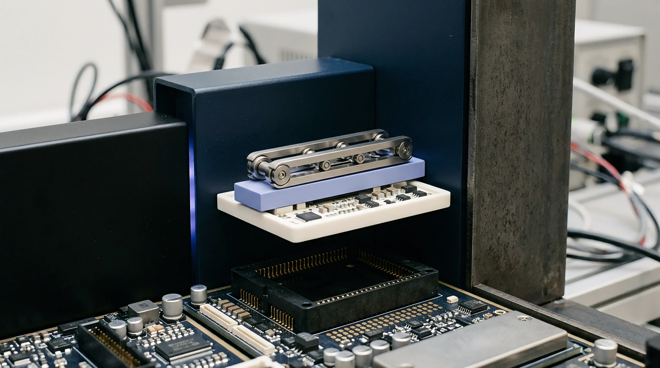
Automated test fixtures lock physical modules into high-frequency RF test sockets to measure output parameters under ambient temperature sweeps. Physical bench inspection of incoming module shipments forms the primary defense against unannounced silicon stepping changes. Sourcing contracts that rely solely on manufacturer certificate of analysis documents expose buyers to undetected field failures.
Clamping the module into a standardized high-frequency test fixture allows automated bench equipment to capture radio frequency spectrum data, current consumption traces, and digital register signatures within sixty seconds per unit.
Automated Bench Verification Protocols
Receiving inspection procedures mandate quantitative evaluation of key physical parameters prior to releasing inventory to production lines. Physical inspection verifies solder mask quality, package markings, and shielding can integrity, but high-frequency RF measurement reveals internal silicon modifications. An automated test station incorporating a vector signal analyzer, a precision DC power analyzer, and a shielded anechoic enclosure measures fundamental RF output power, transmitter error vector magnitude, phase noise, harmonic radiated power, and multi-state current profiles.
- Mount the target radio module into the shielded coaxial test fixture ensuring pneumatic clamping force delivers repeatable ground contact resistance below ten milliohms.
- Apply nominal supply voltage of 3.3 volts DC from a fast-transient precision power source while recording boot-up current transient profiles at a sampling rate of one megasample per second.
- Issue register read commands over SPI or I2C bus interfaces to extract silicon revision identification codes, internal hardware stepping registers, and boot ROM checksum values.
- Execute high-frequency transmitter sweep across low, mid, and high channel assignments at maximum configured output power into a fifty-ohm calibrated load.
- Capture radiated spurious emissions across second, third, and fourth harmonic frequencies inside the shielded enclosure using a calibrated horn antenna and spectrum analyzer.
- Initiate sleep mode command sequence and measure baseline quiescent current consumption after a stabilization period of five seconds.
Acceptance sampling follows international statistical standards. Sourcing contracts specify Acceptable Quality Limit levels under ISO 2859-1 general inspection level II. Critical defects, such as incorrect silicon revision IDs or sleep current spikes exceeding specification limits by fifty percent, trigger zero-acceptance thresholds across the entire incoming lot.
Yield drops instantly.
| Test Parameter | Measurement Unit | Baseline Value | Max Permissible Delta | Sampling Protocol |
|---|---|---|---|---|
| Quiescent Sleep Current | Microamperes (uA) | 1.2 uA at 25C | Plus 0.4 uA deviation | 100 percent automated test |
| Carrier Phase Noise | dBc/Hz at 100 kHz offset | minus 98 dBc/Hz | 3 dB elevation maximum | AQL 0.40 Normal Inspection |
| Second Harmonic Radiated Power | dBm absolute power | minus 42 dBm | 4 dB elevation maximum | AQL 0.40 Normal Inspection |
| Error Vector Magnitude (EVM) | Percent RMS | 2.1 percent | 1.5 percent absolute shift | AQL 1.00 Normal Inspection |
| Synthesizer Lock Time | Microseconds (us) | 140 us | 25 us extension maximum | AQL 0.40 Normal Inspection |
Section 8.4 of the international supply agreement assigns full financial liability for batch rejection testing fees to the component vendor whenever incoming RF metrics deviate by more than three decibels from baseline specification.


Delta
Statistical comparison between golden baseline samples and production lot test data isolates subtle transceiver changes. Quantitative risk assessment requires rigorous mathematical analysis of physical test results to differentiate normal wafer fabrication process variations from unannounced silicon stepping changes. Silicon manufacturing processes exhibit natural statistical distributions across wafer lots.
Gaussian distribution curves describe parameter variations such as threshold voltage, trace resistance, and gate oxide thickness. An unannounced silicon stepping shifts the population mean or expands the variance of these distributions.

Statistical Analysis of Parameter Shifts
Analysis of variance and hypothesis testing quantify the likelihood that an incoming module lot originates from an altered silicon mask set. Sourcing quality teams calculate the Process Capability Index, denoted as Cpk, for critical radio frequency and energy parameters across consecutive incoming shipments. A stable silicon process delivers a Cpk value exceeding 1.33.
When an incoming shipment exhibits a Cpk drop below 1.00, or when the population mean shifts by more than two standard deviations from the established golden baseline mean, an unannounced physical alteration has occurred inside the component.
Quantitative risk allocation frameworks use this statistical delta to trigger mandatory contractual notifications, component holds, and financial cost-recovery mechanisms before non-compliant hardware reaches customer hands.

Which Regulatory Trigger Forces Module Level Recertification?
Permissive changes under regional rules depend on whether an altered radio component alters radiated power levels or occupied bandwidth. Federal Communications Commission regulations dictate that any change in integrated circuit stepping that increases fundamental peak output power by more than 0.5 decibels or increases out-of-band spurious emissions by more than 3.0 decibels requires a formal Class II permissive change filing. European rules under RED Article 3.2 dictate that if harmonic output increases beyond fixed spectral limits, full technical file updates and notified body reviews become mandatory.
- Radiated Output Power Variance Shifts exceeding 0.5 dB require RF exposure re-evaluation and spurious emissions verification.
- Occupied Bandwidth Expansion Any broadening of channel bandwidth exceeding 2 percent triggers immediate regulatory review under FCC Part 15 and ETSI EN 300 328 standards.
- Spurious Harmonic Floor Elevation Radiated emissions increasing by more than 3.0 dB on second or third harmonics invalidate existing test reports.
- Transceiver Clock Source Alterations Internal oscillator changes or phase-locked loop redesigns require frequency stability testing across temperature ranges from minus 40 to plus 85 degrees Celsius.
A statistical shift exceeding two standard deviations in harmonic radiated power across three consecutive production lots indicates an unannounced silicon stepping revision requiring technical file auditing.
When receiver sensitivity drops across multiple operational channels simultaneously, the root cause sits inside the integrated circuit rather than in passive filtering components.


Penalty
Contractual financial damages map physical module variance directly into landed unit cost reductions. Commercial sourcing agreements for multijurisdictional radio components incorporate quantitative risk allocation formulas that transfer financial exposure from the module buyer back to the module supplier. When a supplier ships modules containing unannounced silicon revisions that cause production downtime, re-testing expenses, or regulatory non-compliance, parametric penalty equations determine the precise financial compensation owed to the buyer.

Mathematical Risk Allocation Formulas
Parametric pricing adjustments compute unit price reductions based on measured physical deviations from contractually agreed baseline specifications. If an unannounced silicon stepping increases sleep current consumption, reducing end-device battery service life, the supplier incurs a direct unit price penalty proportional to the energy deficit.
The unit price penalty equation is expressed as:
Penalty = Unit Cost × ( 1 – ( Measured Battery Life / Target Battery Life ) ) × Penalty Factor
Assume a target radio module base cost of 12.50 USD, designed for a target battery life of 120 months. An unannounced silicon stepping increases sleep current, reducing calculated battery life to 90 months. Applying an agreed contract penalty factor of 1.5 yields:
Penalty = 12.50 × ( 1 – ( 90 / 120 ) ) × 1.5 = 12.50 × 0.25 × 1.5 = 4.6875 USD per unit
The adjusted invoice price per module drops from 12.50 USD to 7.81 USD to compensate the buyer for reduced product field viability and increased customer warranty liability.
| Variance Category | Physical Metric | Mathematical Compensation Formula | Commercial Application Threshold |
|---|---|---|---|
| Energy Budget Deficit | Quiescent Sleep Current (uA) | Penalty = Base Price ( (Measured Current – Spec Current) / Spec Current ) 2.0 | Sleep current elevation exceeding 20 percent over spec |
| RF Link Degradation | Receiver Sensitivity (dBm) | Deduction = Fixed Credit per dB ( Measured Sensitivity – Baseline Sensitivity ) | Sensitivity degradation exceeding 1.5 dB across any channel |
| Regulatory Re-testing | Lab Fees and Legal Filings | Indemnity = Direct Lab Cost + Admin Fee (25,000 USD) + Line Halt Charge per Hour | Class II permissive change triggered by unannounced die revision |
| Production Line Downtime | Assembly Halt Hours | Damages = Hourly Line Rate (5,000 USD/hr) Production Interruption Hours | Incoming lot rejection at receiving clamp inspection station |

Liquidated Damages and Line Halt Indemnity
Unannounced silicon revisions that pass initial receiving checks but cause assembly failures or end-of-line test rejections trigger immediate liquidated damage clauses. Contract terms define fixed monetary damages for factory line stoppages. When receiving clamp inspection halts a manufacturing line due to silicon variance, the component vendor pays fixed hourly line halt fees to cover idle factory labor, re-scheduling costs, and delayed product delivery penalties.
Parametric contract clauses automatically adjust component invoice prices based on measured physical performance deltas, transferring financial energy deficit costs directly back to the silicon vendor.
Whether supply contracts can successfully enforce liquidated damages for unnotified silicon revisions without forcing component suppliers to exit high-volume commercial pricing tiers remains an open commercial question.


Remedy
Sourcing practices protect device manufacturers through multi-tiered indemnification provisions and dual-foundry sourcing mandates. Enforcing technical and financial protections requires comprehensive legal and operational remedies integrated into master supply agreements. When an unannounced silicon stepping threatens multijurisdictional market access, buyers deploy contractual mechanisms ranging from escrow accounts and dual-sourcing mandates to total lot rejection and financial indemnification calls.

Contractual Protection Clauses and Escrow Architecture
Master sourcing contracts require explicit definition of mandatory change notification windows. Suppliers must provide written engineering change notices a minimum of one hundred eighty days prior to introducing silicon mask revisions, metal layer adjustments, ROM patches, or process node transitions. The change notice documentation must include full physical test reports across temperature extremes, regulatory delta evaluations, and register mapping updates.
Operational contract terms incorporate the following core protections:
- Hardware Escrow Requirements Suppliers deposit full register-level documentation, boot ROM source code, and analog trim parameters with an independent escrow agent upon contract execution.
- Mandatory Re-Qualification Audit The buyer reserves the right to perform bench validation and regulatory testing on sample quantities at the supplier expense prior to production lot authorization.
- Dual-Foundry Qualification Mandates Primary radio modules must maintain footprint-compatible secondary sourcing options utilizing alternative silicon foundries to prevent supply disruptions during silicon stepping transitions.
- Indemnification Holdback Reserve The buyer retains five percent of total contract value in an escrow holdback account for twelve months to offset latent field failure costs induced by unannounced silicon changes.
- Right of Product Return and Restocking Fee Waiver Rejection of incoming lots based on unannounced silicon stepping variations grants the buyer the right to return all un-assembled inventory for full cash refund with all freight charges paid by vendor.
Establishing escrow accounts for register-map documentation alongside dual-sourcing hardware qualifications protects the buyer against unannounced silicon changes while preserving long-term manufacturing continuity.