Sub-GHz Radio Frequency Synthesizer Crystal Thermal Dissipation Mechanics
Sub-GHz PA power bursts generate micro-Kelvin crystal thermal gradients that shift carrier frequency, demanding thermal isolation and tight TCXO specification.
Gradient
Integrated power amplifiers in sub-gigahertz wireless devices dump heat into silicon substrates during transmit bursts. Radios operating between +14 dBm and +22 dBm draw substantial direct current, turning a large portion of that energy into thermal dissipation right on the transceiver die. Switching topologies in the 433 MHz, 868 MHz, and 915 MHz allocations generate sharp, localized heating within milliseconds.
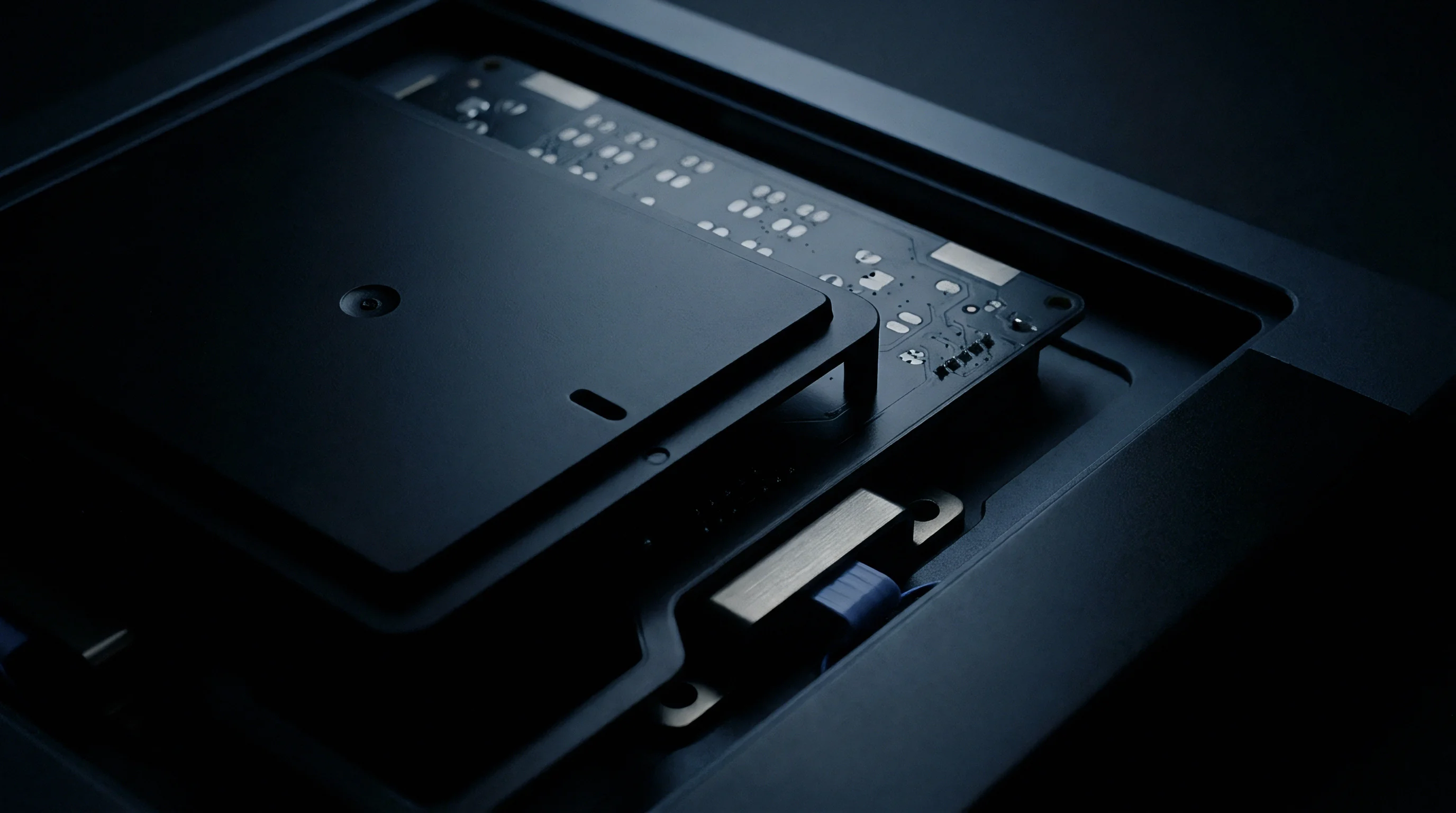
When an amplifier stage sheds several hundred milliwatts, thermal flux spreads outward through the leadframe, epoxy die attach, ground thermal pad, and surrounding printed circuit board copper pours.
A reference quartz crystal placed near the transceiver package absorbs this conducted heat. AT-cut crystal blanks follow a cubic temperature-frequency characteristic, with an inflection point positioned near 25 degrees Celsius. Static shifts follow this curve cleanly, but non-uniform heat spreading creates localized thermal gradients across the crystal package.
Temperature differences between the ends or edges of the blank induce mechanical stress through anisotropic thermal expansion, pulling the resonant frequency before the quartz reaches thermal equilibrium.

High-Power Transmit Dissipation Mechanics
RF output stages operating at twenty-two decibel-milliwatts convert over sixty percent of supplied DC energy into localized joule heating. A transceiver drawing 120 milliamperes from a 3.3-volt supply rail consumes 396 milliwatts of total DC power. Radiating +22 dBm accounts for 158 milliwatts of RF power, leaving 238 milliwatts trapped inside the package as heat.
Junction-to-ground-pad thermal resistance (Rthη JG) in a compact 4×4 mm quad-flat no-leads package runs between 25 and 40 degrees Celsius per watt. During a long transmit packet, silicon junction temperature climbs by 6 to 10 degrees Celsius inside the first 20 milliseconds.
Heat transfer through the board substrate depends on the thermal impedance of the FR-4 dielectric and the cross-section of connecting copper traces. Copper has a thermal conductivity around 385 watts per meter-kelvin, whereas FR-4 conducts only 0.25 to 0.3 watts per meter-kelvin. Continuous ground planes between the transceiver exposed pad and crystal ground terminals act as direct thermal pathways.
Heat travels along the top copper layer, enters the crystal ground pins, and climbs straight into the ceramic package.
A 100-milliwatt thermal pulse at the transceiver ground pad induces a 0.3-degree Celsius temperature differential across a 2016 crystal package within 12 milliseconds.
Thermal Flux Pathways in Integrated Sub-GHz Transceivers
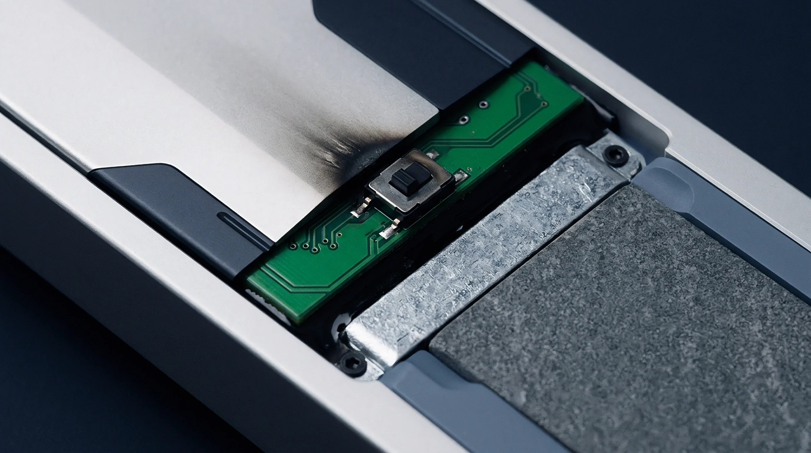
Heat leaves the active silicon junction through conductive leadframes and surface-mount solder balls, branching into three vectors: conduction across board copper, radiation inside the sealed enclosure, and convection across nearby components. In unventilated enclosures, conduction through copper planes accounts for more than eighty-five percent of the heat reaching the quartz crystal. The crystal package ~ typically a 3225, 2520, or 2016 ceramic substrate ~ has an internal base-to-blank thermal resistance (Rthη PB) between 50 and 90 degrees Celsius per watt.
When heat reaches one end of the ceramic substrate first, the package expands unevenly. Conductive epoxy mounting points transfer this strain directly into the crystal lattice, changing acoustic wave velocity in the quartz plate and causing a transient frequency excursion that standard bulk temperature curves do not account for. Ignoring thermal gradient paths between power amplifiers and reference crystals results in unrecoverable carrier frequency offsets, corrupted packet preambles, and field link failures in telemetry hardware.
Pad
Board layout dictates the conduction path between power-dissipating silicon and adjacent frequency references. Protecting a reference crystal from thermal pulses generated by high-power sub-gigahertz radios requires careful handling of copper mass, layer stackups, and substrate thermal vias. Standard routing that prioritizes short trace lengths for high-frequency signal integrity often puts crystal oscillators within 3 to 5 millimeters of the transceiver exposed ground pad, establishing a low thermal resistance link between the heat source and the frequency anchor.
Clearance between the transceiver and the crystal oscillator introduces necessary conductive thermal resistance. FR-4 isolates far better than solid copper, but top and bottom ground pours bypass that isolation whenever solid metal bridges connect the devices. Effective layout demands isolation zones and selective routing that steer thermal energy into dedicated dissipation areas before it reaches the crystal pins.
| Layout Isolation Configuration | Distance to Crystal (mm) | Effective Thermal Resistance (°C/W) | Peak Crystal ΔT at 500 ms Tx (°C) | Max Frequency Excursion (ppm) |
|---|---|---|---|---|
| Direct ground pour connection | 3.5 | 42 | 2.4 | 2.10 |
| Solid pour with 4-via thermal array | 5.0 | 68 | 1.5 | 1.30 |
| Ground relief slot with bridge trace | 8.0 | 135 | 0.7 | 0.55 |
| Dual-layer thermal slotting zone | 12.0 | 240 | 0.3 | 0.15 |
Thermal Isolation Geometry and Ground Plane Slotting
Etching thermal relief slots into ground copper between the transceiver package and crystal pads extends the conductive path without interrupting ground return continuity. A slot routed or etched through top and inner layers forces heat around the cutout, extending the thermal path from 5 millimeters to 20 millimeters or more. This deflection lets heat bleed into wider ambient copper areas, dampening the pulse that arrives at the crystal pads.
Placing an array of plated thermal vias between the transceiver exposed pad and internal ground planes redirects flux away from the surface layer. Heat drops vertically through high-density via arrays into internal copper planes that act as sinks. Spreading thermal energy across inner ground planes before it migrates laterally cuts top-layer thermal gradients near the crystal.
Copper Pour Mass and Substrate Thermal Vias
Solid surface pours provide lateral spreading while plated holes redirect energy into internal reference layers. Heavy copper, such as 2-ounce (70-micrometer) foil, lowers trace resistance but accelerates lateral heat transfer. Balancing thermal management with RF performance requires dedicated copper zoning.
Ground planes directly under the crystal must retain high electrical continuity for RF shielding while remaining thermally decoupled from transceiver output stages.
Board layout revisions that omit designated ground slots or reduce thermal via density beneath a radio module lead directly to carrier offset drift and transient frequency pulling that violate regional spectral mask boundaries during regulatory qualification.

Frequency
RF phase-locked loops depend on stable reference clocks to lock their voltage-controlled oscillators. Sub-gigahertz radios operating with 12.5 kHz or 25 kHz channel spacing under European ETSI EN 300 220 or US FCC Part 15 allocations tolerate minimal absolute frequency error. Synthesizers multiply crystal reference frequencies across wide division ratios to generate outputs in the 169 MHz, 433 MHz, 868 MHz, or 915 MHz bands.
A 26 MHz crystal multiplied to 915 MHz uses a division factor (N) of 35.192, so any fractional parts-per-million drift at the crystal maps directly to the transmit carrier.
A 2.0 ppm thermal shift on a 26 MHz crystal produces a 1.83 kHz offset at 915 MHz. In constant-envelope frequency shift keying (2GFSK or 4GFSK) or chirp spread spectrum (LoRa) modulations, carrier offsets degrade demodulation at the receiver. When the transmit carrier shifts mid-packet, receiver tracking loops can lose lock, causing bit errors and dropped packets.

Synthesizer Loop Filter Dynamics under Crystal Frequency Pulling
Fractional-N synthesizers use phase-frequency detectors and charge pumps paired with analog loop filters to stabilize output signals. The loop filter bandwidth, typically set between 10 kHz and 100 kHz, sets how quickly the phase-locked loop responds to reference changes. If crystal pulling outpaces loop filter settling, the phase detector registers a sharp phase error, causing phase noise spikes and frequency overshoot on the RF output.
Dynamic thermal pulling during power amplifier ramp-up introduces rapid frequency slewing (fracdfdt). If that rate exceeds the loop bandwidth tracking capability, the synthesizer briefly unlocks or runs with elevated phase noise. High phase noise degrades adjacent channel power ratios (ACPR), spilling energy into neighbouring channels and breaching compliance limits.
Synthesizer loop bandwidths below 100 kilohertz fail to track crystal frequency pulling caused by thermal pulses shorter than 5 milliseconds.
What Carrier Offset Floor Destroys Sub-GHz Link Margin?
Receiver channel filters strip out energy falling outside passband limits. When transmitter crystal pulling shifts the carrier off nominal center frequency, offsets exceeding twenty percent of channel bandwidth cause severe attenuation in intermediate-frequency (IF) selectivity filters.
Receiver automatic frequency control (AFC) loops calculate and correct carrier offsets during initial packet preamble bytes. If thermal gradients continue pulling frequency across the payload, the initial AFC correction fails before the packet finishes. This mismatch drives up packet error rates and triggers energy-costly retransmissions.
The exact boundary where dynamic thermal drift overwhelms receiver tracking under elevated ambient temperatures remains an active question in sub-gigahertz mesh network design.
Transient
Temperature shifts across quartz blanks develop within milliseconds during packet transmission. Static frequency-temperature tables stored in flash memory cannot correct transient gradients because onboard thermistors read ambient PCB temperatures rather than instantaneous quartz stress. High duty cycle telemetry or industrial mesh repeating keeps the power amplifier active over long windows, worsening thermal accumulation.
The time constant (τ) of crystal package thermal dissipation falls between 50 milliseconds and 500 milliseconds, governed by package mass and pad geometry. During transmit bursts shorter than 5 milliseconds, heat barely reaches past the outer ceramic. Across bursts lasting several hundred milliseconds, thermal energy saturates the package, driving frequency excursions that peak near the end of the packet.
Thermal Pulse Characterization during High Duty Cycle Transmissions
Continuous transmissions produce an initial steep frequency shift from package strain, followed by slower logarithmic drift as the bulk assembly warms. When transmission stops, the amplifier cools quickly, reversing the thermal gradient and causing secondary frequency overshoot before the component settles back to ambient.
- Mount the target sub-gigahertz radio assembly inside a temperature-controlled thermal chamber set to 25 degrees Celsius ambient baseline.
- Connect the RF output terminal through a 30 dB calibrated coaxial attenuator directly to a high-speed vector signal analyzer or real-time spectrum analyzer.
- Attach a micro-thermocouple or optical infrared thermal probe directly to the ceramic top lid of the reference quartz crystal package.
- Configure the radio transceiver to execute repeated 500-millisecond transmit bursts at maximum output power (+22 dBm) with a ten percent duty cycle.
- Synchronize the spectrum analyzer trigger with the radio transmit enable GPIO signal to capture instantaneous frequency offset versus time at 1-millisecond resolution.
- Record crystal lid temperature simultaneously with carrier frequency excursion to establish the dynamic thermal transfer delay.
- Calculate the dynamic pulling slope (fracdfdt) during the first 50 milliseconds of output power activation.

Worked Calculation for Power Amplifier Thermal Dissipation and Frequency Shift
Consider a 915 MHz transmitter on a 3.3-volt supply. Drawing 130 mA in transmit mode to produce +20 dBm (100 mW) of RF output consumes 429 mW of DC power (3.3 V × 0.13 A). Subtracting the 100 mW RF output leaves 329 mW dissipated as heat inside the transceiver package.
Assuming a total thermal resistance path from junction to crystal base through the ground pour of 85circC/W, the steady-state temperature rise at the crystal base calculates as 0.329 W × 85circC/W = 27.975circC. Over a 300 ms burst, thermal rise reaches roughly twenty percent of that asymptote, or 5.59circC. Applying the AT-cut quartz parabolic coefficient (k = -0.035 p±/(circC)2) around a 25 °C inflection point, warming from 25 °C to 30.59 °C yields -0.035 × (30.59 – 25)2 = -1.09 p±.
At 915 MHz, that -1.09 ppm shift generates a -997.35 Hz carrier offset.
| Modulation Scheme | Channel Bandwidth (kHz) | Transmit Power (dBm) | Dissipated Power (mW) | Max Allowable CFO (Hz) | Thermal Shift Limit (ppm) |
|---|---|---|---|---|---|
| Narrowband 2GFSK | 12.5 | +14 | 110 | 1,250 | 1.36 |
| Standard 2GFSK | 25.0 | +20 | 329 | 2,500 | 2.73 |
| Wideband 4GFSK | 100.0 | +22 | 480 | 10,000 | 10.92 |
| LoRa SF7 / BW125 | 125.0 | +22 | 480 | 31,250 | 34.15 |
| LoRa SF12 / BW125 | 125.0 | +22 | 480 | 12,500 | 13.66 |
Evaluating board thermal time constants against worst-case burst durations keeps peak crystal frequency excursions within half the receiver modulation bandwidth.


Margin
Procurement specifications for radio modules demand clock stability verification under full transmit power. Selection usually balances uncompensated crystals (XTAL), thermistor-integrated crystals (TSX), and temperature-compensated crystal oscillators (TCXO). Standard crystals keep unit costs low (0.12 to $0.25 USD) with zero static power consumption, but exhibit wide drift ($± 10 to ± 30 ppm) over industrial ranges (-40 to +85 degrees Celsius) alongside unmitigated dynamic pulling.
Temperature-compensated crystal oscillators use internal analog networks or ICs to apply correction voltages to a varactor diode, holding drift between ± 0.5 and ± 2.0 ppm. These components raise bill-of-materials costs ($0.45 to $0.90 USD) and draw 1.5 to 2.5 milliamperes of continuous current, which cuts into battery margins.
Compensation Technologies and TCXO Selection Economics
TCXOs adjust varactor diode bias to counter thermal drift curves, with higher-end units incorporating internal thermal insulation or packaging geometries that slow external heat transfer. Thermistor-integrated crystals (TSX) place a sensing element right next to the quartz blank inside the package, allowing the host microcontroller to read crystal temperatures directly and adjust digital frequency synthesizer offsets.
- Frequency Stability Window specifies maximum frequency deviation across the full industrial temperature range (-40 to +85 degrees Celsius) under static ambient conditions.
- Thermal Transient Sensitivity defines the maximum allowable frequency excursion rate (fracdfdt) when exposed to a localized thermal step function.
- Power Supply Rejection Ratio quantifies oscillator output frequency stability against ripple on the supply rail caused by power amplifier switching transients.
- Startup and Settling Time measures the delay from enable signal assertion until the clock output stabilizes within specified frequency accuracy limits.
- Phase Noise Floor establishes maximum allowable phase noise density at 1 kHz and 10 kHz offsets to prevent transmitter selectivity degradation.

Contract Specification Clauses for Oscillator Thermal Immunity
Procurement documents require dynamic thermal verification alongside standard static tolerances. Screening parts only at static room temperature allows poorly decoupled layouts to clear factory testing, only to fail in the field when extended transmit bursts trigger thermal pulling.
- Thermal Transient Limits Clause mandating that total frequency shift during a 500-millisecond transmit burst at maximum output power shall not exceed 1.5 parts per million.
- Layout Thermal Isolation Audit requiring visual trace and ground plane inspection verifying minimum physical keepout clearances and thermal relief slotting.
- Environmental Step Profiling mandating five-point thermal chamber screening across -40, 0, +25, +60, and +85 degrees Celsius with simultaneous transmit power burst activation.
- Component Level TCXO Compliance requiring vendor certification reports confirming thermal hysteresis stays below 0.3 parts per million.
ETSI EN 300 220 compliance limits force sub-GHz transmitters to hold frequency stability within 10 parts per million across the complete operational thermal window.
Standard delivery contracts state that modules failing dynamic carrier offset limits during thermal burst testing shall be replaced at the vendor’s expense under standard warranty provisions.