Meaning
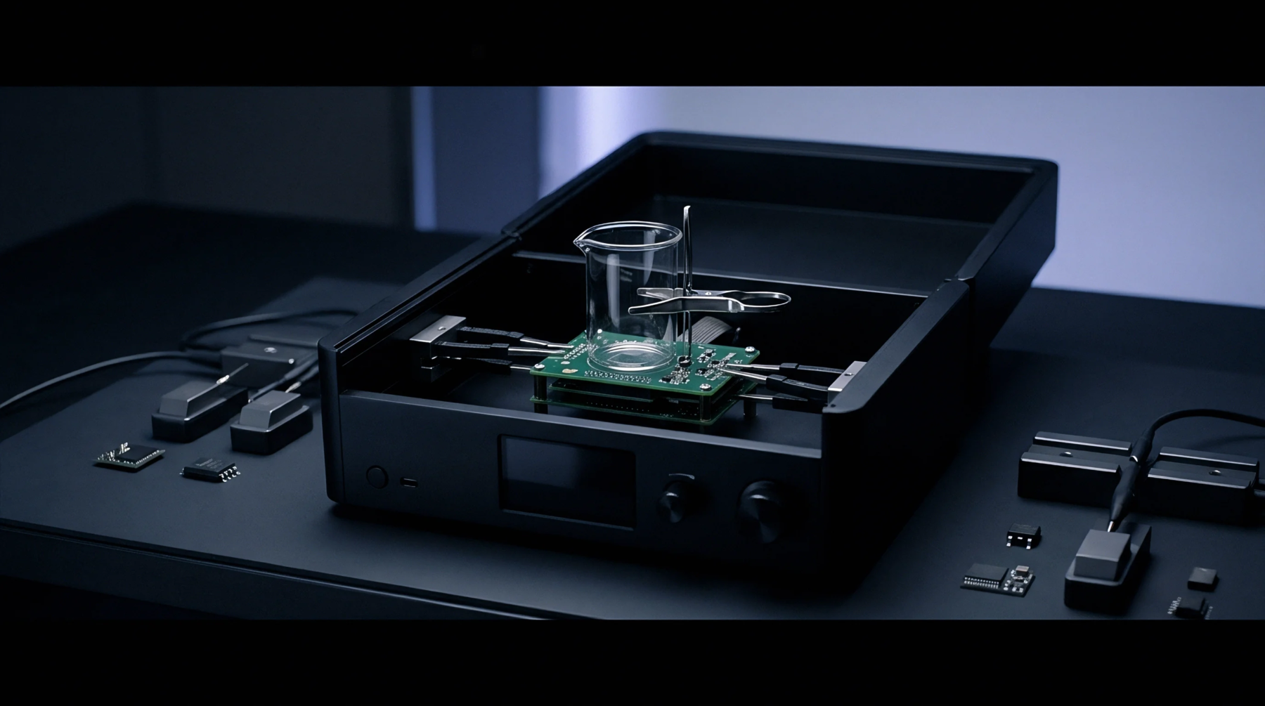
Electromagnetic coupling sensors function as high-resolution inductive or capacitive devices designed to map localized field distributions across printed circuit board surfaces or small radio frequency components. A near field probe captures reactive components of fields before these waves propagate into the far field region, which allows for the isolation of specific emission sources during diagnostic testing. The device terminates in a coaxial connector that feeds signals into a spectrum analyzer for quantification of amplitude and frequency.
Measurements obtained with a near field probe remain sensitive to proximity and orientation, requiring consistent positioning relative to the source under inspection. Precision relies on the small aperture of the loop or dipole tip which rejects interference from distant ambient signals.
Electromagnetic Sensitivity
Operators detect unintentional radiators by sliding the sensor over high frequency traces or integrated circuits during the initial development phases of hardware validation. A near field probe provides sufficient spatial resolution to distinguish between signals from adjacent pins or closely routed transmission lines. The induction loop responds to magnetic field components, while an electric field tip detects potential differences between the probe and a conductive trace.
High fidelity data acquisition depends on maintaining a fixed distance from the assembly during the scan. Proper shielding of the coaxial cable prevents common mode noise from injecting errors into the captured signal stream. Analysis software interprets the raw spectral data to identify which trace acts as the primary contributor to overall electromagnetic interference.
Verification Workflow
Integration labs employ these sensors as part of the formal pre-compliance testing sequence prior to submitting hardware for final certification. Use of a near field probe facilitates the rapid debugging of electromagnetic compatibility failures found during full chamber testing. Engineers document the locations of maximum field strength to determine where board layout modifications or additional filtering components provide the greatest attenuation.
This systematic approach reduces the total time required to bring a device into compliance with international standards by identifying specific layout flaws early in the production life cycle. Quantitative assessment allows teams to establish baseline performance metrics that ensure repeatable results across multiple board revisions.
Component Tolerance
Variations in tip geometry directly affect the coupling factor between the probe and the device under test. Narrow tips provide finer resolution at the cost of reduced signal sensitivity, while larger loops increase output levels at the expense of localized accuracy. Calibration of the test setup requires a stable source to normalize amplitude readings against known reference values.
System performance degrades if the dielectric constant of the probe housing changes or if the metallic tip shows signs of oxidation or wear. Accurate spatial mapping depends entirely on the stability of the probe mount during the measurement cycle. The diagnostic effectiveness of a near field probe remains constrained by the thermal environment of the circuit under load.