Modular Radio Integration Audits for Host Hardware Approvals
Integrating pre-certified radio modules into host hardware requires layout audits, spurious emission pre-scans, and permissive change filings to secure market access.


Frame

Ground Planes and Board Stackup Physics
Integrating a pre-certified radio module into a host device host PCB introduces electromagnetic interactions that alter the module’s baseline radio frequency performance. A modular grant proves compliance only in a standalone reference environment, usually a uniprofboard with defined ground plane dimensions, traces, and power delivery networks. Placing that module onto a multi-layer host mainboard shifts the local dielectric boundary, changes ground reticulations, and alters thermal distribution.
Traces carry high frequencies. When host hardware engineers cut ground planes under the module RF launch area or route high-speed digital lines directly beneath the module shield, parasitic capacitance couples clock noise into the transceiver front-end. Copper area limits heat.
Host board stackup configurations determine whether the integrated module maintains its original output power profile or suffers from parasitic antenna detuning. A continuous, uninterrupted ground reference plane directly below the module top layer suppresses microstrip radiation leakage. Discontinuities in this reference plane force return currents to travel around split gaps, creating slot antennas that radiate at harmonic frequencies of the system baseband clock.
RF trace impedance control requires strict adherence to controlled microstrip or coplanar waveguide geometry. Deviations in dielectric thickness, trace width, or copper weight shift the characteristic impedance away from fifty ohms, creating standing waves that reflect energy back into the module power amplifier.
Ground plane continuity directly under the RF launch point controls return path inductance and prevents board edge radiation.
Metal housings and structural reinforcement brackets near the integrated module alter antenna input impedance and radiation patterns. Physical clearance around internal chip or trace antennas requires minimum spatial separation, typically fifteen to twenty millimeters of clear area devoid of metallic components, battery casings, and display flex cables. Bringing a zinc alloy frame or aluminum heat sink within this reactive near-field region shifts the resonant frequency, lowers radiation efficiency, and increases high-angle side lobes that induce spurious emissions failures during compliance testing.
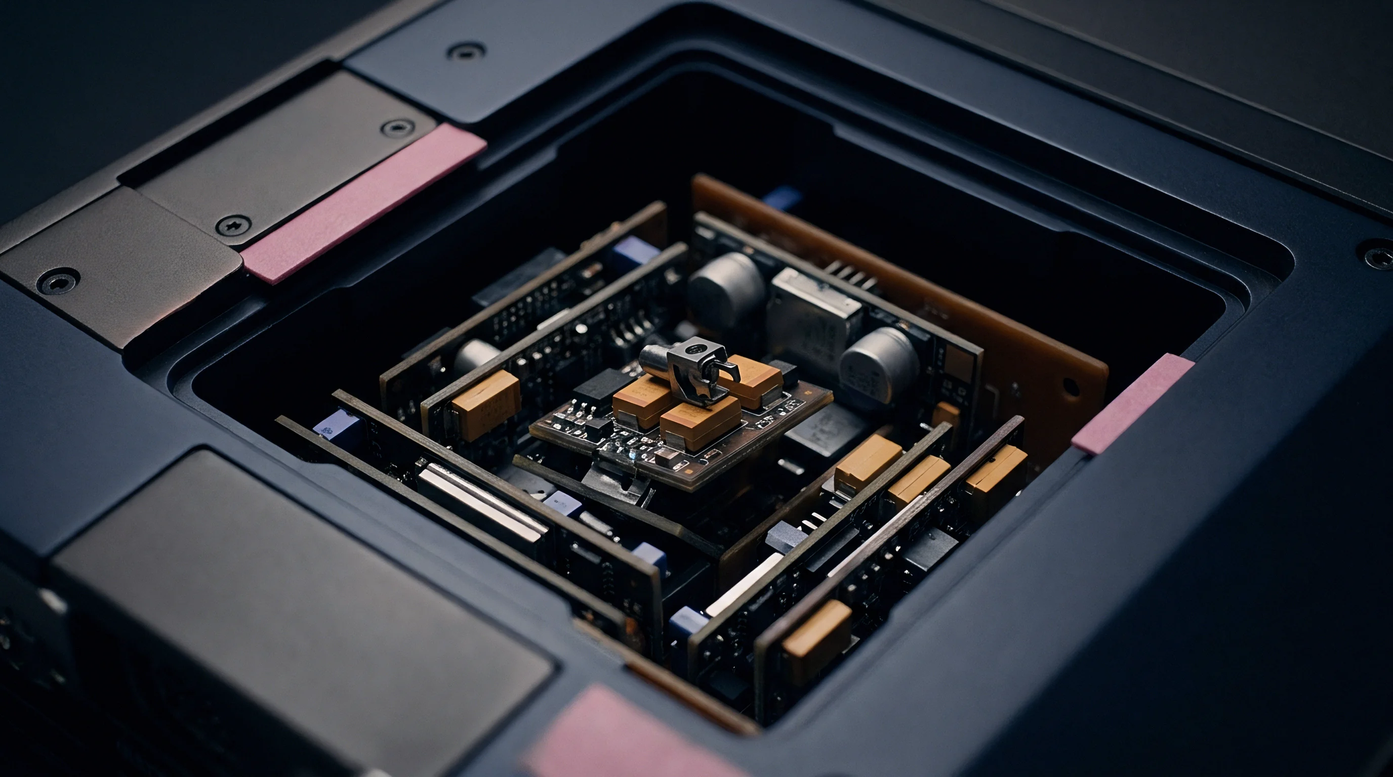
Antenna Trace Layout and Host Coupling
Host layout engineers implementing a modular transmitter with an external antenna connector must match the specific trace design certified by the module manufacturer. Federal Communications Commission rules under Knowledge Database 996369 D02 specify that host manufacturers using trace antenna designs or custom RF microstrip layouts from the modular approval manual must follow those layout parameters exactly. Deviations exceeding specified tolerances in trace width, layer stackup, substrate dielectric constant, or component values invalidate the original modular grant and shift regulatory responsibility to the host integrator.
- Microstrip line mismatch alters transmission line characteristic impedance, driving insertion loss above target thresholds and triggering localized trace heating under continuous transmission.
- Unshielded flex cables passing within the antenna reactive near field pick up carrier frequency energy and re-radiate baseline clock harmonics into spatial chambers.
- Inadequate ground via stitching around coplanar waveguide structures allows parallel plate waveguide modes to propagate through internal board layers, feeding RF noise directly into digital baseband processors.
- Power rail inductance along unpassivated trace runs causes localized voltage droop during peak transmitter power bursts, degrading frequency stability.
Shielding enclosures surrounding the host hardware must incorporate conductive gasket perimeter seals or tight via-stitched ground walls to isolate noisy digital processing units from sensitive radio receivers. Host hardware integration audits begin at the physical layout layer, inspecting layer stackup artwork, trace impedance calculations, and ground plane continuity before any operational testing commences. Failure to replicate the host layout guidance prescribed in the modular grant conditions forces full intentional radiator testing on the host assembly.
Solid mechanical fastening prevents microphonic resistance variations across structural ground contact points. Plastic enclosures with vacuum-metallized conductive coatings present aging risks, as mechanical flexure cracks the thin metallic layer over thermal cycles, introducing micro-gaps that behave as non-linear junctions under strong ambient RF fields. The structural housing acts as an extended antenna structure, radiating noise generated internally by high-speed memory interfaces, switching regulators, and display driver clocks.
Host hardware integration succeeds when layout engineers treat the boundary between the module pins and the host PCB as a high-frequency transmission system rather than a DC signal path. Antenna placement requires isolation from onboard switching noise sources, particularly step-down converter inductors operating above one megahertz. Mechanical tolerances in assembly fixtures dictate whether structural ground spring fingers establish low-impedance contact with chassis metalwork or introduce variable contact resistance that shifts radiated emissions profiles across manufacturing lots.

Spill
Host Noise Sources and Receiver Desensitization
Radiated spurious emissions and receiver desensitization represent the primary physical failure modes encountered during host hardware integration audits. Host digital electronics generate continuous-wave narrowband interference and broadband impulsive noise across broad spectral bands. High-speed processor buses, serial interfaces such as Peripheral Component Interconnect Express and Universal Serial Bus, switched-mode power supplies, and unshielded display drive lines radiate noise that enters the module antenna or feeds into its power supply pins.
Receiver desensitization occurs when host-generated noise raises the noise floor of the integrated radio receiver, reducing operational sensitivity and throughput without necessarily exceeding regulatory radiated emission limits.
Noise masks weak signals. Characterizing this degradation requires measuring the host receiver noise floor with the system powered in various operational states compared to a quiet baseline with host processors dormant. Power rail ripple on host mainboards represents a primary vector for conducted noise transfer into the radio module.
Linear regulators or dedicated ferrite filtering topologies are necessary on module supply tracks to prevent high-frequency ripple from modulating the voltage-controlled oscillator, which creates sideband spurious emissions that violate European Telecommunications Standards Institute European Norm 300 328 spectral mask criteria.
| Host Peripheral Noise Source | Primary Harmonic Frequency Band | Observed Peak Noise Delta | Receiver Sensitivity Impact | Mitigation Circuitry Required |
|---|---|---|---|---|
Harmonic multiplication within non-linear host components turns low-frequency system clocks into problematic microwave radiation. A two-hundred-megahertz bus clock generates its twelfth harmonic at 2.400 gigahertz, falling directly into the Industrial, Scientific, and Medical frequency band. Antennas radiate near metal.
When this harmonic aligns with the operating channel of an integrated Wi-Fi or Bluetooth radio, the transmitter output amplifies the clock noise, driving spatial radiation above regulatory emission thresholds defined in Federal Communications Commission Part 15 Subpart C Section 15.209.

Radiated Spurious Emissions in Enclosed Housings
Enclosing the integrated module inside a physical host product creates cavity resonance conditions that concentrate electromagnetic energy at specific frequencies. These spatial standing waves alter the effective isotropic radiated power of both the intended transmission and unwanted harmonic emissions. Radiated spurious emissions testing evaluates the fully assembled product across three-dimensional space inside a semi-anechoic or fully anechoic chamber, rotating the host on a motorized turntable while sweeping a measurement antenna over height ranges from one to four meters.
A two-decibel increase in host power supply ripple can raise transmitter harmonic spurious emissions past absolute class B radiated limits in semi-anechoic chamber sweeps.
Absorber material configuration inside the test chamber isolates the direct path signal from reflection artifacts, ensuring precise signal strength readings. If internal host wiring or cable harnesses pass near the integrated radio antenna, high-frequency energy couples onto those passive conductors, turning them into secondary radiating structures. Ferrites reduce high harmonic noise.
System audits identify these parasitic radiating paths by comparing preliminary conducted emissions at the module antenna port against full three-dimensional spatial radiated scans of the complete product assembly.
Shielding tabs reduce radiated spill. When testing uncovers harmonic spikes exceeding Class B limits, hardware engineers must install localized grounding absorbers, add board-level shielding cans, or re-route internal high-speed ribbon cables away from the radio module enclosure zone. Identifying these spatial leakage paths early in the host hardware audit prevents late-stage mechanical tool re-definitions, preserving both product launch dates and compliance margins.
Ignoring host-generated noise during initial design validation leads to chamber re-test loops that consume hardware budgets and stall commercial market availability.

Filing

When Does Host Hardware Layout Trigger Full Filing Updates?
Modular approvals permit host integrators to reference the module’s original filing data, avoiding full radio certification testing for every new host application. Regulatory authorities establish distinct operational boundaries governing when this reference model remains valid and when explicit filing updates are required. Under Federal Communications Commission rules, host integration requires adherence to the modular grant conditions regarding RF exposure limits, antenna gain parameters, and co-location restrictions.
Unapproved changes invalidate radio grants.
If a host integrator selects an antenna of the same type (such as a planar inverted-F antenna) with equivalent or lower directional gain than the antenna authorized on the module’s original grant, no formal filing update is needed, provided spatial separation distances are maintained. Replacing the certified antenna with a higher-gain alternative or a different antenna family (such as swapping a monopole for a patch antenna) alters the spatial radiation distribution and peak equivalent isotropically radiated power, requiring a Class II Permissive Change filing under Federal Communications Commission Part 2 Section 2.1043.
| Regulatory Jurisdiction | Primary Regulatory Standard | Antenna Swap (Equal Gain) | Antenna Change (Higher Gain) | Co-Located Transmitters Added |
|---|---|---|---|---|
European Union Radio Equipment Directive 2014/53/EU mandates that host manufacturers assume total legal responsibility for final product conformity. Integrating a pre-certified radio module into a host device does not automatically confer compliance upon the combined equipment. The host integrator must perform an assessment against the essential requirements of Article 3.2, verifying that the radio spectrum is used efficiently and without harmful interference.
This evaluation includes spot-checking radiated spurious emissions, occupied bandwidth, and out-of-band emissions to confirm that host digital circuitry has not compromised module radio compliance.

Permissive Changes and Multi Transmitter Co Location
Integrating multiple pre-certified radio modules into a single host hardware platform (such as combining a Cellular 5G module with a Wi-Fi 6E transceiver and a Bluetooth Low Energy radio) introduces complex co-location compliance requirements. Federal Communications Commission rules define co-located transmitters as two or more radios operating simultaneously within twenty centimeters of each other or within the same host hardware enclosure. Intermodulation products generated by non-linear mixing of transmitted signals create distinct spurious radiation frequencies not present when either radio operates individually.
- Evaluate spatial separation distances between all integrated module antennas inside the host chassis to determine if SAR evaluation or simultaneous transmission MPE calculations apply.
- Perform simultaneous transmission intermodulation pre-scans across all operating frequency bands to detect non-linear mixing products exceeding maximum spurious limits.
- Compile combined MPE or SAR ratio calculations demonstrating that the cumulative exposure ratio remains below unity across all simultaneous transmit modes.
- Document software lock controls preventing non-evaluated operational state combinations, ensuring high-power modes cannot execute simultaneously on overlapping frequencies.
- Submit required Class II Permissive Change filings or Technical Approval Certificate amendments through a Telecommunications Certification Body or Notified Body.
Federal Communications Commission KDB 996369 D04 Section 3.2 specifies that simultaneous transmission intermodulation products must be evaluated with all co-located radios transmitting at maximum output power.
Under Japanese Radio Law administered by the Ministry of Internal Affairs and Communications, co-located radios integrated into host equipment require formal technical attestation reviews if simultaneous operation creates intermodulation interference in restricted radio frequency bands. Similarly, South Korea’s National Radio Research Agency requires updated registration filings when host integration alters the operational environment of previously certified radio modules. Formal documentation must explicitly detail the antenna properties, host shielding mechanisms, and simultaneous transmission controls that preserve environmental radio standards.
Federal Communications Commission KDB 996369 D04 Clause 4.1 establishes that host manufacturers using modular approvals remain strictly liable for ensuring final assembly compliance with all intentional and unintentional radiator rules.


Bench

Test Firmware Configurations and Transmit Modes
Executing an effective host hardware radio integration audit requires specialized test firmware to control the integrated module outside its normal application stack. Standard production firmware dynamically adjusts output power, changes operating channels, and enters low-power sleep cycles based on network traffic. Compliance verification requires static, repeatable radio operational states where the transmitter runs continuously at maximum rated output power, maximum duty cycle, and fixed single frequencies across low, mid, and high channels within each operating band.
Module vendors must supply dedicated regulatory test software or direct asynchronous AT command interfaces that bypass higher-layer protocol drivers. Ground pins suppress loop currents. This firmware allows test engineers to configure specific modulation schemes, set carrier frequency offsets, activate direct sequence spread spectrum or orthogonal frequency division multiplexing modes, and disable dynamic frequency selection mechanisms during test sequences.
Operating the module via direct driver hooks allows precise measurement of conducted output power and spectral mask fidelity directly at the micro-coaxial test port on the host PCB.
Verification test software must lock the module into continuous-wave or highest-duty-cycle packet modes to capture worst-case thermal and radiated interference profiles.
System power rails must be monitored throughout high-duty-cycle test runs to confirm that host voltage regulators maintain stable voltage levels without thermal throttling or excessive voltage ripple. Voltage droop under maximum RF output power induces phase noise in the module synthesizer, broadening the main transmission lobe and bleeding energy into adjacent channels. Board trace mismatches alter power.
Radiated tests conducted with unstable host power supplies risk false failures that stem from power system collapse rather than genuine radio hardware non-compliance.

Radiated Emissions Audit Execution
Full chamber audits walk through a systematic verification sequence designed to isolate host digital noise from true radio modular non-compliance. Preparing the host sample involves attaching high-frequency semi-rigid coaxial pigtails to the RF output pins, bypassing internal antennas for conducted baseline checks before placing the fully assembled unit into anechoic measurement environments.
- Configure the host device with specialized regulatory test firmware and establish direct serial interface access to issue radio control commands.
- Perform conducted power measurements across all supported frequency channels and modulation schemes to confirm baseline parity with the module grant data.
- Position the fully assembled host unit on an elevated non-conductive turntable inside a semi-anechoic test chamber at three-meter or ten-meter measurement distances.
- Activate host digital processing units, display screens, high-speed memory buses, and peripheral interfaces to simulate maximal operational noise profiles.
- Command the integrated module to transmit continuously at maximum power on the lowest operating channel of the operational band.
- Rotate the turntable through three hundred sixty degrees while sweeping the measurement antenna height from one to four meters in both horizontal and vertical polarizations.
- Identify, log, and categorize all radiated emission peaks, distinguishing host digital clock harmonics from intentional transmitter output and intermodulation products.
- Repeat spatial rotational sweeps across mid and high operating channels, applying peak, quasi-peak, and average detection modes in accordance with ANSI C63.4 and ANSI C63.10 standards.
When radiated emissions exceed target limits, test engineers apply localized near-field probe sweeps over the host mainboard surface to pinpoint exact leakage sources. High-frequency magnetic field probes identify switching inductors, unshielded processor cores, and PCB edge gaps emitting intense localized fields. Applying conductive copper tape, localized absorbing foam, or additional ground via connections provides immediate physical diagnostic confirmation before permanent PCB layout modifications are committed to production tooling.
The module vendor stated that the integrated radio would pass host compliance automatically because the module held full modular certification.
Field failures halt customs shipments.


Ledger

Chamber Schedule Allocations and Retest Buffers
Host hardware approvals represent significant schedule lead time and financial expenditure in product commercialization schedules. Compliance costs accumulate through accredited laboratory chamber access fees, engineering labor, specialized test sample preparation, and regional filing tariffs levied by telecommunications certification bodies. Unplanned re-testing caused by unexpected host emissions failures drains development budgets and delays commercial shipments, forfeiting market advantages and triggering contractual late-delivery penalties.
Booking semi-anechoic chamber time at accredited independent laboratories requires advance operational planning, as chamber availability often demands lead times of four to eight weeks. Test plans must incorporate structured time buffers to accommodate on-bench troubleshooting and physical host modifications when initial pre-scans reveal unexpected harmonic emissions. Performing preliminary pre-compliance scans on lower-cost local engineering benches or non-accredited pre-compliance facilities mitigates financial exposure before committing to full accredited compliance sweeps.
| Compliance Phase | Required Test Samples | Average Chamber Hours | Direct Laboratory Costs | Projected Lead Time |
|---|---|---|---|---|
Retests cost real laboratory time. Staging international compliance filings sequentially or concurrently alters total landed compliance costs. Leveraging mutual recognition agreements simplifies filing procedures across primary markets, but local representation rules, specific labelling regulations, and in-country sample testing requirements in markets such as South Korea, Brazil, or China introduce schedule dependencies that must be managed alongside primary domestic approval trajectories.

Financial Metrics of Host Access Compliance
Direct compliance expenditures represent only a portion of the overall cost model. Analyzing financial exposure requires calculating the revenue loss associated with delayed market launch windows, sample hardware destruction costs during extreme environmental or surge tests, and engineering re-work overhead required to rectify layout deficiencies late in the product development cycle.
- Direct laboratory fees cover accredited chamber utilization, test engineer labor, technical report generation, and formal Telecommunications Certification Body filing processing fees.
- Local in-country agency representation covers mandatory legal representation, document translation, local administrative handling, and annual certificate maintenance fees.
- Engineering sample destruction losses account for hardware samples modified, soldered, stressed, or structurally altered during severe RF testing protocols.
- Commercial delay penalties quantify lost gross margin per week of delayed market availability set against fixed overhead and inventory holding costs.
Consider a practical host hardware deployment scenario involving an industrial gateway integrating a pre-certified 5G cellular module. Assuming a production volume of fifty thousand units over a two-year product lifecycle, budgeting thirty thousand dollars for host integration testing, Class II Permissive Changes, and European Union RED technical file construction yields a amortized compliance cost of sixty cents per unit. Conversely, if an un-audited host hardware design fails a customs entry sweep due to non-compliant radiated spurious emissions, the financial impact includes seized inventory, full market recall costs, mandatory field retrofits, and comprehensive accredited re-testing expenses exceeding one hundred fifty thousand dollars.
Completing a comprehensive compliance dossier requires assembling specific technical artifacts that validate the host integration boundary. Hardware engineering practices must systematically compile layout documentation, test reports, and administrative forms to satisfy regulatory audit requirements across target markets.
- Complete schematic documentation detailing host power distribution networks, high-speed digital buses, filter circuits, and module interface pins.
- PCB stackup artwork files detailing layer thickness, dielectric parameters, copper weights, and controlled impedance microstrip layout traces.
- Accredited test reports documenting conducted power, occupied bandwidth, radiated spurious emissions, and co-location intermodulation scans.
- Signed declarations of conformity identifying host manufacturer legal liability, applied standards versions, and module grant integration compliance.
- User instruction manuals containing mandatory regulatory statements, RF exposure warnings, host packaging mark layouts, and external housing label artwork.
The financial metrics governing host radio integration dictate that regulatory compliance must be treated as a core design parameter rather than a post-development administrative step. Early investment in physical layout validation, pre-compliance chamber scans, and systematic dossier creation protects capital investments and ensures immediate market access across global regulatory jurisdictions.
Whether regional regulatory authorities will establish harmonized multi-transmitter co-location evaluation rules that eliminate redundant per-host permissive change filings across international trade borders remains an open question for global product practices.