Buying a Ready Module against Building a Custom One
Selecting between ready modules and custom builds requires balancing upfront non-recurring costs and regulatory testing against long-term serial unit margins.


Scope
Choosing between a pre-certified radio module and a discrete layout establishes how engineering work is split between an internal team and outside vendors. It determines who handles high-frequency RF routing, who submits regulatory filings, and who carries financial exposure if assembly yields drop. Each integration level operates as a contract scope under commercial shorthand ~ either shifting upfront engineering expense into unit costs or trading custom board space for a faster market launch.
These integration choices shift landed cost structure directly.
Turnkey modules integrate the RF IC, matching network, crystal oscillators, and bandpass filter into a single shielded surface-mount package. Vendors complete intentional radiator certifications under FCC Title 47 CFR Part 15, RED Directive 2014/53/EU, and ISED RSS-247 prior to distribution. Solder-mounting that module onto a host carrier board allows the buyer to leverage those existing filings, narrowing local compliance scope to unintentional radiator testing under FCC Part 15 Subpart B. This eliminates three to six months of laboratory testing and reduces execution risk, though it increases unit bill-of-materials costs across production runs.

Engineering Allocation across Integration Tiers
Semi-custom modules adapt an existing reference design to fit specific host dimensions, connector layouts, or thermal constraints set by the buyer. The module supplier adjusts board outlines, repositions peripheral components, or retunes passive antenna matching networks while preserving the core System-on-Chip design and shield enclosure. The buyer pays targeted non-recurring engineering charges for artwork modifications, mask generation, and partial re-testing without funding a complete radio development program.
Signal integrity remains the vendor’s obligation, provided the host board follows specified keep-out boundaries and power rail noise limits.
Reference designs return layout responsibility and component sourcing to the host engineering team. Silicon vendors supply schematics, suggested bills of materials, and recommended PCB land patterns as uncertified starting points. Working from a reference design requires internal engineers to replicate high-frequency trace geometries, match dielectric layer stackups, and route power distribution without performance guarantees from the vendor.
The buyer assumes full responsibility for regulatory approvals, factory testing, and production yields, trading supplier markup for execution risk.
Custom discrete designs eliminate pre-packaged templates entirely to minimize board footprint, unit BOM expense, and current draw. Operating at this level requires deep internal expertise in microstrip design, impedance matching, harmonic filtering, and multi-layer stackups. Engineers select discrete silicon, microcontrollers, passives, crystals, and shielding cans individually.
This yields the lowest piece cost at high volumes, but demands hundreds of engineering hours, dedicated RF instrumentation, and full certification across every target market.

Non-Recurring Costs and Unit Economics
Costs divide into initial development expenses and serial unit pricing. Non-recurring engineering covers schematic capture, board layout, antenna simulation, test fixture development, lab bookings, and line setup. Turnkey module suppliers absorb these expenses into their standard product development, spreading them across millions of off-the-shelf units.
The buyer avoids direct NRE fees, paying instead a higher unit price that incorporates vendor margin, licensing, and certification recovery.
Amortization structures often obscure true unit margins.
Semi-custom contracts bill NRE directly for panelization modifications, SMT stencils, and targeted radio requalification. These upfront charges typically range from fifteen thousand to seventy-five thousand dollars depending on whether revisions alter the RF shield, layer stackup, or trace geometries. In return, unit costs drop ten to twenty-five percent below catalog module pricing, establishing a clear volume threshold where upfront engineering outlay pays off.
| Integration Level | Upfront NRE Range | Relative Unit Cost | Design Lead Time | Regulatory Scope | IP Ownership |
|---|---|---|---|---|---|
| Turnkey Module | $0 – $5,000 | 100% (Baseline) | 1 to 4 Weeks | Unintentional Radiator Only | Vendor Proprietary |
| Semi-Custom Module | $15,000 – $75,000 | 75% – 90% | 8 to 16 Weeks | Permissive Change / Re-test | Shared / Application Specific |
| Reference Design | $40,000 – $120,000 | 50% – 70% | 16 to 26 Weeks | Full Intentional Radiator | Buyer Owns Layout |
| Custom Discrete | $100,000 – $300,000+ | 35% – 55% | 26 to 52 Weeks | Full Intentional Radiator | Buyer Owns Everything |
Reference designs and custom discrete implementations require significant initial capital for board spins, laboratory testing, and automated test fixtures. Compliance testing at accredited facilities costs twenty-five thousand to sixty thousand dollars per regional band (FCC, CE, ISED, MIC). A custom discrete design easily accumulates over one hundred fifty thousand dollars in engineering labor, prototype iterations, and testing before the first volume unit leaves the factory floor.

Break-Even Volume Arithmetic
Determining where a custom layout becomes more cost-effective than a pre-packaged module requires weighing upfront fees against unit component savings. At ten thousand units, a turnkey Wi-Fi 6 and Bluetooth 5.3 module costs around $8.50. The raw silicon, passives, crystal, and filter for a custom BOM sum to $3.20 ~ a component savings of $5.30 per unit.
However, that custom build carries $180,000 in initial costs: $110,000 in engineering labor, $40,000 in certification fees, and $30,000 in production test development.
Dividing $180,000 by the $5.30 per-unit savings yields a break-even point of 33,962 units. Below that threshold, lower overall capital expenditure favors the turnkey module. Above 34,000 units, cumulative unit savings eclipse the initial development outlay.
At 100,000 units, going discrete reduces net manufacturing costs by over $350,000 after fully writing off development expenses.
Buyers consistently underestimate peripheral board space expenses and regulatory re-certification delays when calculating discrete engineering economics. A turnkey module occupies a known physical footprint with guaranteed RF isolation. Moving that circuitry onto the mainboard often forces stackup expansions from four layers to six to accommodate ground planes and impedance-controlled signal traces ~ adding twelve to eighteen percent to bare board fabrication across the product’s lifespan.
Section 8.2 of the master engineering services agreement transfers all financial liability for non-compliant unintentional emissions back to the buyer if the host board layout deviates from the module vendor’s printed ground-plane guidelines.
Contractual ambiguity triggers costly disputes during bring-up and factory qualification. Statements of work must outline explicit deliverables, test parameters, and file formats rather than relying on broad commercial summaries. Leaving technical boundaries undefined leads to unplanned expenses, stalled production lines, and contested invoices.
Vague scope definitions repeatedly surface as operational failures during manufacturing bring-up:
- Unassigned Antenna Tuning Scope occurs when neither side assumes responsibility for tuning the RF stage to the enclosure, leaving the product with weak range and failed compliance sweeps.
- Missing Board Support Package Source leaves software developers unable to adjust low-level drivers, halting integration when peripheral silicon revisions land.
- Unfunded Compliance Re-Testing hits buyers when host board changes invalidate modular certifications, forcing unplanned laboratory spending.
- Undefined Factory Calibration Rights locks the buyer out of internal RF power registers, blocking automated output tuning on the assembly line.
- Omitted Component End-Of-Life Liabilities exposes the buyer to sudden supply cutoffs when chipmakers discontinue discrete silicon without advance warning.
Financial projections that ignore scrap rates, warranty reserves, and extra layout spins distort unit economics. A thorough comparison accounts for yield differences between factory-screened modules and discrete SMT components placed directly on the main line. Module suppliers test before shipping.
Populating discrete RF parts directly onto a host board transfers component placement losses to the main assembly, where a single defective passive can ruin an expensive board.
Tooling retention fees can escalate quickly.
A forty-two thousand dollar invoice for host board PCB panel redesign and compliance laboratory re-testing occurred when a semi-custom supplier altered their substrate pin layout by 0.8 millimeters without providing updated mechanical drawings three months prior to serial pilot runs.


Stack
Silicon vendor reference designs reflect idealized circuits evaluated under controlled laboratory conditions. They assume infinite ground planes, noiseless power rails, and ideal thermal dissipation ~ conditions that rarely exist in production products. Engineers transferring a reference design onto a crowded host PCB must carefully evaluate every passive selection, layer stackup, and driver dependency to keep the radio functional.
Pin density alters these trade-offs significantly.
Evaluation boards rely on thick copper, generous trace clearance, and high-end dielectrics like Rogers 4003C to isolate high-frequency signals. Commercial host boards usually run on lower-cost four-layer FR4 whose dielectric constant shifts with temperature and operating frequency. Swapping Rogers material for standard FR4 drops trace impedance from fifty ohms down to forty-two unless trace widths and layer spacing are recalculated.
A five-ohm mismatch at the antenna feed reflects RF energy back into the power amplifier, cutting range and generating excess heat under the shield.

Evaluation PCB Assumptions versus Production Reality
Reference schematics select passive components to maximize bench performance rather than to optimize unit costs or supply chain availability. They frequently call for ultra-low ESR capacitors, tight-tolerance inductors (+/- 1%), and temperature-compensated crystal oscillators (TCXOs). Replacing specified industrial X7R or NP0 components with standard commercial X5R passives (+/- 20% tolerance) introduces frequency drift and power supply ripple that can unlock the phase-locked loop (PLL) in high-density modulation schemes like 1024-QAM.
| Design Parameter | Silicon Reference Design | Production Host Reality | Performance Consequence |
|---|---|---|---|
| PCB Substrate | Rogers 4003C / High-Tg FR4 | Standard Tg FR4 | Impedance shifts +/- 8%; increased RF insertion loss |
| Layer Stack-Up | 6-Layer Dedicated Ground Planes | 4-Layer Shared Routing/Ground | Increased ground noise; degraded receiver sensitivity |
| Passive Tolerances | 0402/0201 Tight Tolerance (+/-1%) | 0603 Standard Tolerance (+/-10%) | Filter center frequency shifts; harmonic distortion |
| Crystal Oscillator | +/- 10 ppm TCXO Dedicated | +/- 20 ppm Standard Crystal | Frequency drift across thermal cycling; drop-outs |
| Power Supply Ripple | < 10 mV Low-Noise LDO | < 50 mV High-Efficiency Buck | Phase jitter on RF synthesizer; spurious emissions |
Power distribution on reference boards relies on dedicated planes and multi-stage LC filters to deliver clean DC to sensitive analog RF blocks. Routing that design onto a compact host board often forces shared traces with switching regulators, digital microcontrollers, and motor drivers. High-frequency noise from buck converters couples directly into the low-noise amplifier (LNA) power rail, degrading receiver sensitivity by up to twelve decibels and cutting effective range by more than half.
Thermal dissipation creates another hard constraint.
Analysis of power plane decoupling networks on a failed reference implementation revealed high-frequency switching noise from a host buck regulator coupling directly into the chip’s internal phase-locked loop, causing random packet dropping during peak transmission bursts.

What Triggers a Mandatory Layout Revision?
Thermal limits, mechanical enclosure constraints, and power supply ripple frequently disrupt planned component layouts. Enclosing a radio in metal or carbon-reinforced plastic shifts near-field radiation patterns, forcing adjustments to the impedance matching network. The 3-component Pi-network from the evaluation board must be re-tuned using a vector network analyzer (VNA) to restore fifty-ohm impedance at the enclosure boundary.
Trimming the host PCB ground plane compromises the antenna return path. Trace antennas designed for evaluation boards expect a continuous ground plane of at least 40 mm by 40 mm adjacent to the feed point. Reducing that ground plane to fit a compact enclosure lowers antenna efficiency, shifts resonance, and radiates noise through the chassis.
Fixing the issue requires adding lumped tuning components or redesigning the trace antenna geometry, forcing extra PCB revisions and delaying bring-up.
Silicon errata regularly derail layout assumptions late in the development cycle. Chipmakers publish errata documenting hardware bugs, such as internal crosstalk between high-speed serial buses and analog RF inputs. Resolving these issues often requires pull-up resistors, added ground shielding, or rerouting SPI and SDIO clock lines away from the RF front end.
Ignoring silicon errata prior to layout leads directly to non-functional prototypes and forced board spins.

Firmware Driver Maturity and Vendor Libraries
Hardware reliability depends heavily on vendor software stacks. Board Support Packages (BSPs) and SDKs provide low-level drivers, protocol stacks, and peripheral abstraction layers, but software quality varies widely between vendors. A vendor offering low-cost silicon may bundle poorly documented, closed-source driver binaries that crash under heavy interrupt loads or fail to wake reliably from low-power sleep modes.
Closed-source driver binaries prevent engineering teams from diagnosing hardware lockups. When crashes occur inside a pre-compiled stack, engineers cannot inspect registers or apply direct patches. The team becomes reliant on vendor Field Application Engineers (FAEs).
If that vendor prioritizes high-volume Tier-1 accounts, smaller customers can wait months for critical fixes, stalling product launches.
Without source access, the driver binary remains locked.
System firmware stability depends on driver source availability, as closed binary blobs prevent memory corruption analysis during unexpected stack overflows.
Open-source drivers built on established frameworks ~ such as Linux mac80211 or Zephyr RTOS wireless stacks ~ provide complete source code visibility. Teams using open-source drivers can debug memory leaks, refine power management, and patch security vulnerabilities directly. Evaluating software licensing, driver maturity, and repository commit history is just as critical as measuring RF sensitivity or power consumption during hardware selection.
Vector network analyzer sweeps demonstrated that internal power-rail brownouts ~ caused by unbuffered register writes in locked driver binaries ~ were responsible for field resets, rather than host ground noise.


Jig
Manufacturing verification converts engineering designs into volume production. Moving to mass production requires automated test fixtures, calibrated instrumentation, and clear quality standards. Deciding between a pre-tested module and a custom discrete design determines where production testing occurs, who develops the test fixtures, and who absorbs assembly scrap.
Factory capability dictates the operational burden.
Turnkey modules arrive at assembly facilities fully tested and calibrated. The vendor verifies frequency offset, transmit power, receiver sensitivity, and spurious emissions on automated test benches before tape-and-reel packaging. The contract manufacturer treats the module like any standard SMT component during placement and reflow.
Quality inspection focuses on solder joint integrity and basic continuity, avoiding complex RF test gear on the host assembly line.
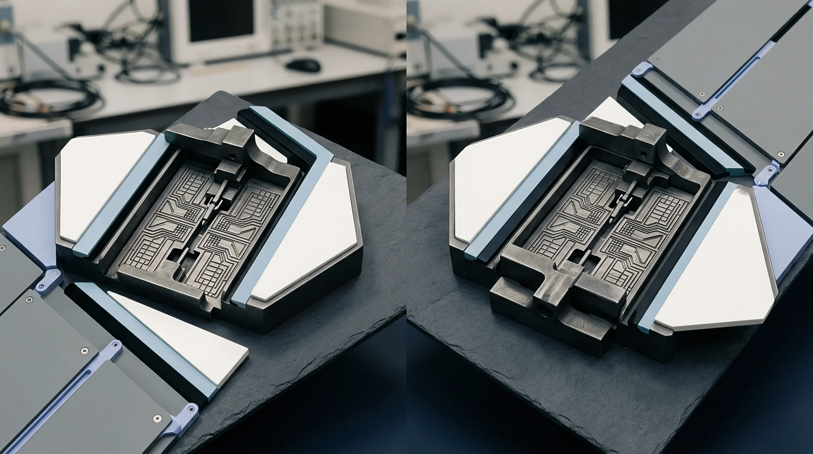
Production Test Fixtures and Bed of Nails Architecture
Custom automated test benches use spring-loaded pogo pins aligned to test pads on the host board. Building a bed-of-nails fixture for a discrete radio requires mechanical tooling, interface PCBs, and pneumatic Faraday boxes for RF shielding. The fixture routes high-frequency signals to spectrum analyzers, signal generators, and power meters, running automated scripts that measure transmit power, EVM, and frequency tolerance on every unit.
Developing production test fixtures requires substantial capital and engineering time. A multi-site RF bed-of-nails fixture equipped with pneumatic clamps, RF switches, and automated test software runs twenty-five thousand to sixty thousand dollars per station. High-volume production requires duplicate fixtures to prevent line bottlenecks.
The buyer must fund fixture construction, calibrate instruments against golden units, and maintain test scripts throughout the product lifecycle.
| Testing Metric / Asset | Turnkey Module Host Line | Custom Discrete Host Line |
|---|---|---|
| Test Fixture Complexity | Simple Functional / Boundary Scan | Complex RF Bed-of-Nails + Faraday Box |
| Instrumentation Assets | Basic Digital Multimeter / JTAG Programmer | Vector Signal Analyzer, Power Meter, Spectrum Analyzer |
| Capital Outlay per Line | $3,000 – $8,000 | $30,000 – $85,000 |
| Test Execution Time | 5 to 15 Seconds per Board | 45 to 120 Seconds per Board |
| RF Calibration Required | No (Pre-calibrated at module factory) | Yes (Frequency offset & power tables written to Flash) |
| Assembly Yield Risk | Low (Scrap limited to SMT placement) | High (Scrap includes defective discrete RF components) |
Yield drops quickly when RF parameters drift.
Logging thermal drift during continuous transmission sweeps confirmed that uncalibrated internal oscillators caused a 14% drop in line yield when ambient factory temperatures exceeded 32 degrees Celsius during summer production runs.
Incoming Inspection and Quality Acceptability Criteria
Modules arriving at the factory undergo statistical sampling to verify solder joint quality and packaging integrity. Quality engineers inspect incoming lots against IPC-A-610 Class 2 or Class 3 standards, checking castellation solder joints, coplanarity, and shield seating. Sampling follows ISO 2859-1 (ANSI/ASQ Z1.4) standards to enforce Acceptable Quality Levels (AQL) across critical, major, and minor defect categories.
Establishing explicit incoming quality criteria prevents operational disputes between the buyer, contract manufacturer, and module vendor. A standard sampling plan sets an AQL of 0.4 for critical defects (non-functional RF, shorted pins), 1.0 for major defects (solder voiding over 25%), and 2.5 for minor visual flaws (tarnished plating). Crossing a rejection threshold allows the buyer to reject the lot and return defective reels for full credit or rapid replacement.
Custom discrete designs move quality control down to individual piece parts. The factory receives ICs, passive reels, crystals, and bare boards, placing hundreds of components in a single assembly pass. A defect in any individual component ~ or a solder bridge on an 0201 passive ~ ruins the entire host assembly.
Repairing dense boards requires manual rework stations, skilled technicians, and micro-X-ray inspection, increasing scrap costs and lowering yield.

Factory Yield Variance and Defect Remediation
First-Pass Yield (FPY) directly dictates the net cost of building in-house. On a production line running pre-tested modules, FPY typically exceeds 98.5%. Defect rates remain low because the complex RF front end arrives pre-screened, leaving only standard SMT assembly issues like tombstoning or solder bridges.
Discrete RF builds experience lower initial yields, typically 91% to 95% during pilot and early production runs. Failures stem from passive component tolerances, crystal frequency drift, solder paste variations under micro-BGAs, and tight RF matching margins. A four-point drop in First-Pass Yield on a volume run quickly offsets component cost savings, as scrapped mainboards carry expensive application processors, memory, and power management ICs with them.
Factory qualification requires strict validation timing.
Qualifying a second contract manufacturer for custom discrete assembly requires a structured validation process:
- Fabricate fifty bare PCB panels at the secondary factory using original Gerber X2 or IPC-2581B data and verify stackup tolerances.
- Procure BOM components exclusively through authorized distributors to keep gray-market silicon out of the supply chain.
- Run a pilot batch of twenty-five assemblies on production SMT lines and inspect solder quality with automated optical inspection.
- Run automated boundary scan tests and flash initial bootloader firmware using primary factory bed-of-nails fixtures.
- Place pilot boards into automated Faraday chambers to run transmit power, frequency offset, and EVM test scripts across operating temperatures.
- Perform high-temperature operating life (HTOL) burn-in testing at 85 degrees Celsius for 168 hours on five units to identify early failures.
- Compare secondary factory test data against primary line baselines using statistical process control metrics (Cpk > 1.33).
Following this qualification sequence maintains parity across build sites, protecting product quality and supply continuity.
Section 4.3 of IPC-A-610G Class 2 mandates that bottom-only surface mount terminations on radio module castellations shall exhibit a minimum side overhang of no more than 25 percent of the termination width.
Relying on clear soldering acceptance standards prevents subjective disputes between quality inspectors and process engineers on the assembly floor.
According to the contract manufacturer’s failure analysis report, solder voiding beneath the central thermal ground pad exceeded thirty-five percent because stencil apertures were not segmented into a windowpane pattern as specified on the hardware land pattern drawing.


Custody
Transferring hardware production from a design house or module vendor to an independent plant requires full ownership of technical deliverables. A complete transfer package includes native design source files, fabrication outputs, firmware repositories, and test specifications necessary to build and maintain the hardware independently. Without native CAD files and source code, the buyer remains dependent on a single supplier.
Standard Gerber outputs alone are insufficient for full ownership.
Contracts must specify native CAD source deliverables rather than post-processed fabrication outputs. Gerber RS-274X files and NC drill lists allow a board house to etch raw PCBs, but prevent internal engineers from re-routing traces, updating footprints, or replacing obsolete parts. Full ownership requires native CAD schematics and layout files from Altium Designer, Cadence Allegro, or KiCad.

Complete Design Transfer Package Deliverables
Complete transfer packages pair native CAD databases with thorough fabrication and assembly documentation. Modern formats like IPC-2581 Version B or Gerber X2 bundle layer stackups, copper weights, dielectric constants, target impedances, and drill tables into a single machine-readable package ~ eliminating vendor misinterpretations and accelerating secondary line setup.
Bill of Materials documentation must specify exact Manufacturer Part Numbers (MPN), package footprints, and verified alternates. Generic descriptions such as ’10uF 0603 Capacitor’ allow contract manufacturers to substitute cheaper alternatives that can degrade circuit performance. A production BOM requires an Approved Vendor List (AVL) defining primary and secondary sources for every passive, crystal, connector, and active IC.
Full source code ownership fundamentally shifts risk.
Firmware transfers require full repository access: uncompiled C/C++ source code, build scripts, linker configurations, BSPs, and environment setup documentation. Providing only pre-compiled binaries (.hex or.bin) allows a factory to flash boards, but prevents future software updates, bug fixes, or security patches. Deliverables must require reproducible build environments ~ such as containerized Docker scripts ~ enabling internal developers to compile bit-for-bit identical production binaries.
| Deliverable Artifact | Turnkey Sourcing | White-Label Agreement | Custom Design Transfer |
|---|---|---|---|
| Schematics & Layout Files | None (Vendor Proprietary) | PDF Only / Gerber Output | Native Source Files (Altium/Allegro) |
| Bill of Materials (BOM) | Module MPN Only | Partial (Key ICs Redacted) | Complete MPN List + AVL Alternates |
| Fabrication Output Data | None | Standard Gerber RS-274X | IPC-2581B / Gerber X2 + STEP 3D |
| Firmware Deliverables | Pre-compiled API / SDK | Locked Binary / Signed Image | Full C/C++ Source + Build Scripts |
| Test Equipment & Scripts | Vendor Proprietary Test Line | Vendor Retained Fixtures | Complete Jig Drawings + Source Code |
| Second-Source Transfer Rights | No (Sole Source Supplier) | Restricted by Exclusivity | Unrestricted Global Transfer Rights |
Including exact file manifest requirements directly within early development contracts is essential, as recovering native CAD files from a reluctant design partner after final payment is nearly impossible.

Intellectual Property Rights and Contractual Lock-In
White-label module agreements frequently grant exclusive sales rights while withholding schematics, firmware source code, and complete BOMs. Under this structure, the supplier retains background IP, manufacturing control, and supply chain leverage. The buyer markets a rebranded module while assuming full exposure to the supplier’s financial health, lead times, and price adjustments.
Single-source dependencies leave hardware programs vulnerable. If a sole-source supplier encounters component shortages, factory shutdowns, or insolvency, the buyer lacks the means to move assembly elsewhere. Replacing a proprietary module requires six to twelve months of redesign, board layout, re-certification, and firmware porting ~ costing market share and missing delivery windows.
Development contracts must explicitly divide background IP from foreground IP generated under funded engineering work. Agreements should clearly state that layout artwork, schematics, mechanical CAD models, test scripts, and custom firmware funded via NRE become the buyer’s exclusive property upon invoice settlement. Securing full IP ownership allows the buyer to transition production to alternate contract manufacturers without incurring royalty fees or legal disputes.

Second-Source Qualification and Exit Mechanics
Qualifying a secondary manufacturing facility mitigates single-source supply risks. Dual-sourcing requires secondary tooling, line qualification, and parallel component supply chains. While turnkey modules cannot be dual-sourced at the module level due to proprietary designs, host boards built with discrete layouts can be qualified across multiple contract manufacturers simultaneously.
Component lifecycle tracking and Part Change Notifications (PCN) follow standards such as JESD46, which mandates that vendors provide 90 days’ written notice before altering silicon, wafer fabrication sites, assembly facilities, or packaging. Working with suppliers that adhere to JESD46 protects buyers from unannounced changes that could invalidate certifications or alter circuit behavior.
Verifying a design transfer dossier before final sign-off means confirming specific technical items:
- Native Schematic Source Files must open without missing library parts or broken nets in the specified CAD tool.
- Intelligent PCB Fabrication Outputs in IPC-2581B or Gerber X2 formats must contain full layer stackups, drill tables, and controlled-impedance targets.
- Uncompiled Firmware Source Code must build in a clean environment to produce binary hashes identical to production images.
- Mechanical 3D CAD Assembly Models in STEP or IGES formats must match physical dimensions, connector positions, and keep-out clearances.
- Automated Test Fixture Schematics and executable test scripts must contain documentation enabling independent engineers to replicate factory calibration.
- Authorized Component AVL Lists must list verified part numbers and active second-source alternatives for all semiconductors and passives.
Securing full ownership of design files, test gear, and source repositories turns engineering IP into a corporate asset, preserving supply chain control and long-term margins.
The contract manufacturer’s legal representative stated that while native schematic artwork would be released upon contract termination, all automated test fixture software scripts and factory calibration algorithms remained proprietary trade secrets of the assembly plant under their standard terms of service.
What specific financial covenants and technical audit milestones must a hardware brand write into a master manufacturing agreement to guarantee that a primary contract assembly factory hands over calibrated bed-of-nails test fixtures and uncompiled functional test scripts when production volumes double and force the bring-up of a secondary manufacturing site?